The coating layer of PCB Assembly should be transparent and evenly cover the printed board and components. Whether the coating layer is uniform, to a certain extent, and coating method, it will affect the appearance of the printed circuit board surface and corner part of the coating condition. Components that are impregnated in THE process of SMT will have a "deposit line" of paint accumulation or a small number of bubbles on the edge of the board, which will not affect the function and reliability of the coating layer.
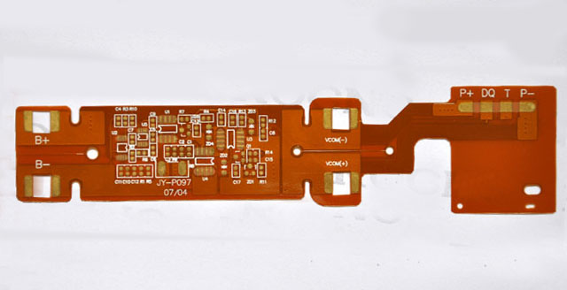
How to check the quality of PCBA shape coating

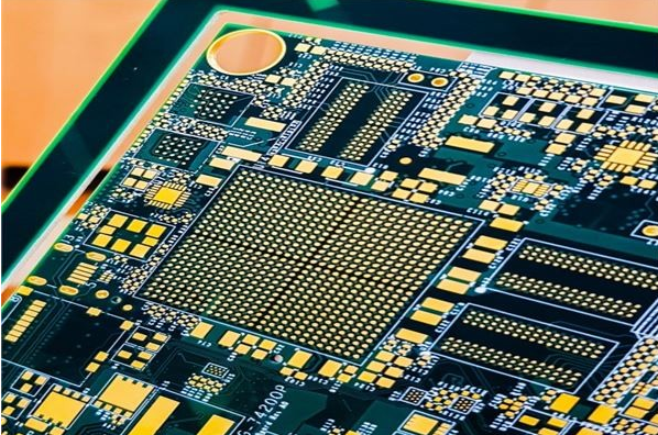
Two, coating layer
The coating layer on the PCB can be visually inspected. Coatings with fluorescent materials can be examined in dim light, and white light can be used as an auxiliary means of coating inspection.
(1) Objectives
. Good adhesion on PCBA components; No cavitation or bubbles.
. No submoisture, powder, peeling, wrinkles (non-attached area) cracking, ripple, fish eye or orange peel off by PCBA detection.
. No inclusion of foreign impurities; No discoloration or transparency reduction; The coating is completely cured and uniform.
(2) Acceptable
. The coating layer is completely cured, uniform and consistent; Areas requiring coating are covered by coating; No adhesion to solder resistance layer.
. There is no adhesion loss, void or bubble, sub-moisture, crack, wavy lines, fish-eye or orange peel peeling at the adjacent bonding pad or conductor surface on PCB; Foreign matter does not affect the electrical clearance between elements, pads or conductor surfaces.
. Thin coating, but can still cover the edge of the component.
(3) Defects
. Coating layer is not cured (showing viscosity)
. Areas requiring coating are not coated.
. Coating is missing in areas requiring coating.
. Adjacent conductor or PCB pad due to apparent adhesion loss (powdery), void or bubble, semi-wet, crack, ripple, fish eye or orange peel off, so that the surface of the pad or adjacent conductor bridge, exposing the circuit or influence element pad or conductor surface gap. Discoloration or loss of transparency.
Three, the thickness of the shape coating layer
The sample can be made of the same material as the PCBA printed board or other non-porous materials, such as metal or glass. Wet film thickness measurement is also a method of coating thickness measurement, which is based on the known dry/wet film thickness conversion relationship to obtain the final coating thickness.