What are the benefits of multilayer printed circuits, which fields and applications?
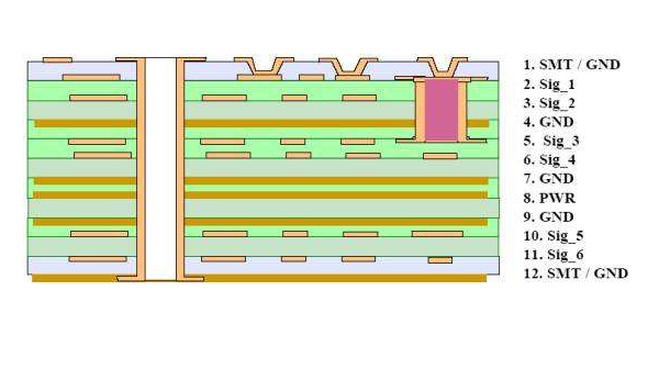
According to its name, a multilayer printed circuit board cannot be called a multilayer printed circuit board. The circuit board includes 2 layers, 6 layers, 8 layers, etc.
Of course, some concepts are composed of three or five circuit layers, which are circuit boards called cards. Multilayer printed circuit.
A larger wire pattern than a double-layer card is separated on the insulating substrate between the layers.
After each wiring layer is printed, each wiring layer is carried out on the basis of support.
Then open a path between each wire layer. The advantage of multi-layer printed circuit boards is that the circuit can be distributed in multi-layer wiring, so that more accurate products can be designed.
Or smaller products can be obtained through multilayer boards. For example: portable telephone circuit boards, micro projectors, recorders and other products with relatively important volumes.
In addition, multilayer technology can improve design flexibility, better control differential impedance and unipolar impedance, and improve the output of certain frequencies of the signal.
Multilayer circuit boards are the inevitable result of the development of electronic technology to high speed, multi-function, large capacity and small volume.
With the continuous development of electronic technology, especially the wide and comprehensive application of large-scale and large-scale integrated circuits, multilayer printed circuits have rapidly expanded to high-density, high-precision, and high-level digitization.
In order to meet the market demand, some limited projects were proposed, a small open permeability, high orifice plate openness and other technologies.
Due to the need for high-speed computers and the aerospace industry, it is necessary to further increase the density of packaging and reduce the size of separate components and the rapid development of microelectronics.

Reduction and reduction. Due to existing space constraints, it is impossible to further increase the assembly density of single-sided printed cards. Therefore, it is necessary to consider using more printed circuits instead of using double-layer boards.
This creates favorable conditions for the emergence of multilayer printed circuit boards. The above content is the analysis and summary of the printed circuit board manufacturer's circuits for more than 10 years. Of course, there is no mention of multilayer printed circuit boards in this article.
High-density PCB strategy
With the reduction of the scale of portable electronic products and printed circuit boards and the reduction of printed circuit boards, users are faced with the problem of solving the difference between traditional printed circuit boards and high-density interconnections.
Semiconductor packaging technology is the main reason for the continuous progress of HDI, but these differences may be greater than the size of the interconnect density.
Semiconductor packaging Although the development of integrated circuit packaging has eased the difficulty of circuit routing, the goals of miniaturization and performance are not easy to achieve.
Because the design process of printed circuits is more complicated, many companies provide multi-functional or multi-functional semiconductor packages, and the number of E/S must be greatly increased while reducing the size and spacing of contacts.
Part of the reason for the increase in E/S and the reduction in spacing is that OEM manufacturers must improve performance in the ever-decreasing space. Questioning the traditional concept of PCBs, some companies have abandoned all or part of the traditional semiconductor packaging.
For example, housing systems quickly entered the main market segments of the market, including public electronics, mobile phones, automobiles, computers, networks, communications, and electronic medical care.
SIP has different advantages in each part of the market, but they have several things in common: relatively short, lower scale and lower cost.
The effectiveness of "zones" (more functions in a single enclosure) has been used in the field of public electronics.
This mixed SIP mode is very common in small-scale systems, such as mobile phones, memory cards and other portable electronic products, and its number is increasing rapidly.
On the other hand, developers usually start to buy uncovered naked chips for installing refurbished chips.
Although the original chip was initially considered a relatively low E/S chip, it can be used for commercial purposes after reorganizing the contact positions on the chip to obtain a more uniform arrangement.
Regarding the mounting of the rotating chip, the connection between a part of the chip and the printed circuit is usually through an alloy bag or an alloy ball.
For the application of supercritical pitch, although the contact point of the copper pillar is small, it is compatible with the traditional convolution brazing process.
Achieve higher circuit density
In many applications, the cost of high-density printed circuit boards is high.
Although the complexity of PCBs is increasing, the price of IDH is falling, and experts predict that this price will continue to fall.
This is partly due to increased competition in the sector, but mainly due to continuous improvements in the manufacturing process and control of the use of materials.
Technological improvements include more effective imaging capabilities, improved chemistry in chemical etching and electroplating, as well as substrates and higher lamination methods.