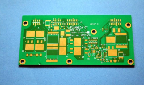
Common sense of high frequency PCB wiring (7)
1. How does Mentor's PCB board planning software handle the differential line team?
After Mentor software defines the characteristics of the differential pair, the two differential pairs can be routed together to strictly ensure that the differential pair line width, distance and length are different, and can be actively separated when encountering obstacles, and the via method can be selected when changing layers.
2. On a 12-layer PCB board, there are three power layers 2.2v, 3.3v, and 5v. The three power supplies are made on one layer. How to deal with the ground wire?
Generally speaking, the three power supplies are built on the third layer, which is better for signal quality. Because it is unlikely to show the signal cross-plane layer cutting phenomenon. Cross-cutting is a critical element that affects signal quality, and simulation software generally ignores it. Regarding the power layer and the ground layer, they are equivalent to high-frequency signals. In practice, in addition to considering the signal quality, the power supply plane coupling (using adjacent ground planes to reduce the power plane communication impedance), layered symmetry, are all factors that need to be considered.
")
3. How to check whether the PCB meets the planning process requirements when it leaves the factory?
Many PCB manufacturers have to pass the power-on network continuity test before the PCB processing is completed to ensure that all connections are correct. At the same time, more and more manufacturers are also choosing x-ray tests to check some problems in etching or laminating. Regarding the finished product board after patch processing, ICT test is generally selected for viewing. This requires adding ICT test points during PCB planning. If there is a problem, it can also be checked by a special X-ray device to see if the processing cause is faulty.
4. Is "the protection of the organization" the protection of the chassis?
Yes. The case should be as close as possible, use less or no conductive materials, and be grounded as much as possible.
5. Is it necessary to consider the esd problem of the chip itself when selecting a chip?
Whether it is a double-layer board or a multi-layer board, the area of the ground should be increased as much as possible. When choosing a chip, consider the ESD characteristics of the chip itself. These are generally mentioned in the chip description, and even the functions of the same chip of different manufacturers will be different. Pay more attention to the planning and consider it comprehensively, and the function of the circuit board will be guaranteed. However, the problem of ESD may still appear, so the protection of the organization is also appropriate and important to the protection of ESD.
6. When making PCB boards, in order to reduce interference, should the ground wire form a closed sum method?
When making the PCB board, generally speaking, the loop area should be reduced to reduce disturbance. When laying the ground wire, it should not be arranged in a closed manner. It is better to arrange it in a branch shape, and it is necessary to increase as much as possible. The area of the earth.
7. If the emulator uses one power supply and the PCB board uses one power supply, should the grounds of the two power supplies be connected together?
It is of course better if you can choose a separate power supply, because it is not easy to cause interference between power supplies, but most equipment has specific requirements. Already the emulator and the PCB board use two power supplies. According to my idea, they should not share the ground.
8. A circuit consists of several PCB boards, should they share the same ground?
A circuit is composed of several PCBs, most of which require a common ground, because it is not practical to use several power supplies on top of a circuit after all. But if you have specific conditions, it will of course be less disturbing to be able to use different power sources.
9. Plan a handheld product with LCD and metal shell. When testing ESD, you cannot pass the ICE-1000-4-2 test. CONTACT can only pass 1100V, and AIR can pass 6000V. In the ESD coupling test, the level can only pass 3000V, and the straight can pass the 4000V test. The CPU frequency is 33MHZ. Is there any way to pass the ESD test?
Hand-held products are also metal cases, so the ESD problem must be more obvious, and LCD may also show more undesirable phenomena. If there is no way to change the existing metal materials, it is advisable to add anti-electricity materials inside the organization, strengthen the ground of the PCB board, and find a way to ground the LCD. Of course, how to do it depends on the specific situation.
10. When planning a system with DSP and PLD, which aspects should be considered for ESD?
As far as the general system is concerned, the parts directly touched by the human body should be considered first, and proper maintenance should be carried out on the circuit and the organization. As for how much impact ESD will have on the system, it depends on different situations. In a dry environment, the ESD phenomenon will be more serious, and the more sensitive and delicate system will have a relatively significant impact of ESD. Although sometimes the ESD impact of a large system is not significant, it is still necessary to pay more attention when planning and try to prevent problems before they occur.