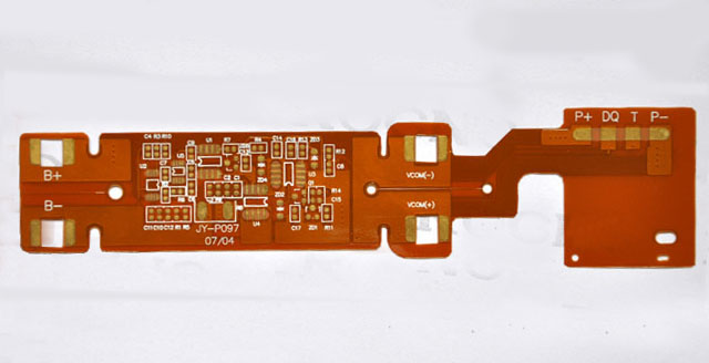
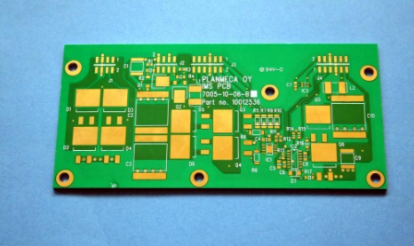
Circuit boards are needed when designing electronic products. The circuit boards of circuit board manufacturers can be divided into single-sided boards, double-layer boards and multi-layer boards according to the number of layers. Generally, double-layer boards are used more often, and elements can be placed on both sides. The device is also very cheap. Like ordinary electronic products, industrial control electronics, sensors, etc., all use double-layer boards. But for many miniaturized products and high-speed products, multi-layer boards are used. Taking mobile phones as an example, it is estimated that 40% or six-layer boards are sufficient for feature phones and elderly phones many years ago, but it is more and more powerful for intelligent In terms of machine, at least eight-layer boards start.

Why do circuit board factories use multi-layer PCB boards? What should be paid attention to when designing multi-layer boards
Why use multi-layer boards
Requirements for product miniaturization.
Today's electronic products are moving closer to miniaturization, but there are not many chips and components used. The PCB should be as small as possible under the premise that the components can be placed. As a result, the PCB cannot be routed, and the area can only be exchanged by the number of layers. .
High-speed signal integrity requirements.
Now that electronic technology is so advanced, products such as routers, mobile phones, switches, and base stations are all high-speed signals, which are susceptible to interference and crosstalk. A reasonable design of multilayer boards can effectively improve signal integrity and minimize signal interference.
What to pay attention to when designing multilayer boards
When a circuit board factory designs a multilayer board, the first issue to pay attention to is the distribution of each layer, which is directly related to the performance of the product.
For a two-layer board, the signal, power and ground wires are crossed together, but for a multi-layer board, this is very particular about it.
How to allocate each layer.
For example, there are multiple distribution methods for four-layer boards, such as 1 signal layer, 2 power layer, 3GND layer, 4 signal layer or 1 power layer, 2 signal layer, 3 signal layer, 4GND layer. The general distribution principle is as follows: signal layer Adjacent to the GND layer plays a role of shielding interference. The tight coupling between the power supply layer and the GND layer is conducive to the stability of the power supply.
Do you want the negative film method?
The so-called negative film method is that the entire plane is a piece of copper, and walking a line is to cut the copper, which is very different from the usual wiring. The usual wiring is the wire. This kind of negative film method is more commonly used in the power layer and GND layer, which is what is often said about the division of the inner electric layer.
The design content of the multilayer board is very much, you can consult the information based on the simple description above.