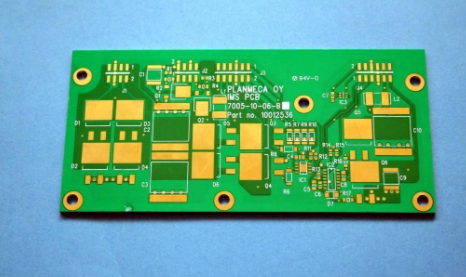
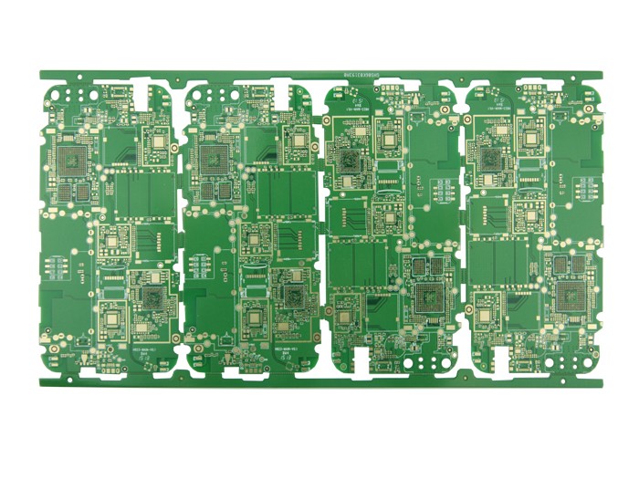
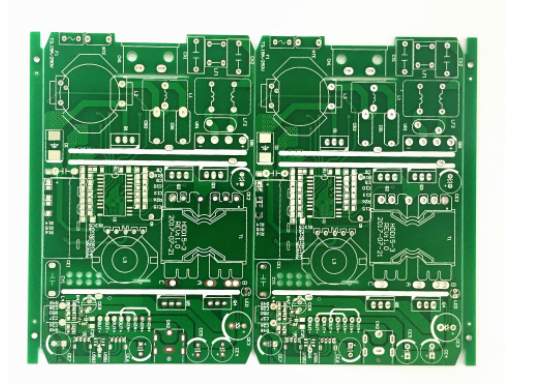
With the development of PCB boards to high-level and high-precision, the accuracy requirements for inter-layer alignment have become more and more stringent, and the problem of PCB layer deviation has become more and more serious. There are many reasons for the PCB layer deviation of the circuit board factory. Now I will share with you a few main factors affecting the layer deviation.

General definition of PCB layer deviation:
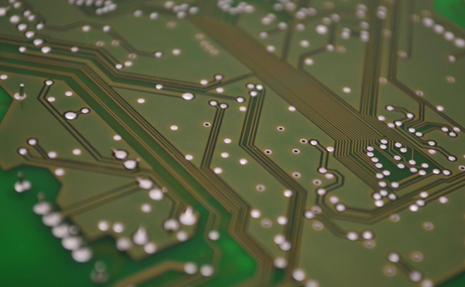
Layer deviation refers to the difference in concentricity between the layers of the PCB that originally requires alignment. The scope of its requirements is controlled according to the design requirements of different PCB board types. The smaller the distance between the hole and the copper, the stricter the control is to ensure its conduction and overcurrent capability.
Commonly used methods to detect layer deviation in the production process:
At present, the method commonly used in the industry is to add a group of concentric circles at the four corners of the production board, set the spacing between the concentric circles according to the requirements of the production board layer deviation, and pass the X-Ray inspection machine or X-drill during the production process. The drone checks the deviation of the concentricity to confirm its layer deviation.
Analysis of the causes of PCB layer deviation:
1. Reasons for inner layer deviation
The inner layer is mainly the process of transferring the graphics from the film to the inner core board, so the layer deviation will only be generated during the graphics transfer production process. The main reasons for the layer deviation are: inconsistent expansion and contraction of the inner film, exposure machine Factors such as misalignment, improper operation during the alignment of personnel and exposure.
Second, the reason for the PCB board pressing layer deviation
The main reasons for the bias of the laminated layer are: the inconsistency of the expansion and contraction of the core plates of each layer, poor punching and positioning holes, fusion dislocation, riveting dislocation, and sliding plates during the pressing process.
The above is an introduction to the problem of PCB board layer offset. Ipcb also provides PCB manufacturers and PCB manufacturing technology.