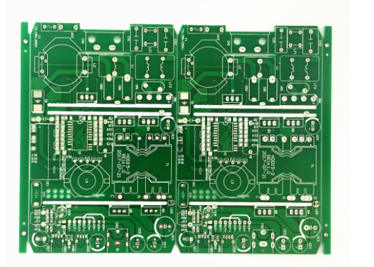
Circuit board factory: OSP process description
OSP is the abbreviation of Organic Solderability Preservatives. It is translated as Organic Solderability Preservatives in Chinese. It is also called copper protector. Simply put, OSP is to chemically grow a layer of organic film on the clean bare copper surface. This film has Anti-oxidation, thermal shock resistance, moisture resistance, to protect the copper surface of the circuit board from oxidation or sulfidation in a normal environment; but in the subsequent welding high temperature, this kind of protective film must be easily removed by the flux quickly, So that the exposed clean copper surface is immediately combined with the molten solder into a strong solder joint in a very short time.

1. Principle: An organic film is formed on the copper surface of the circuit board, which firmly protects the surface of fresh copper, and can also prevent oxidation and pollution at high temperatures. OSP film thickness is generally controlled within 0.2-0.5 microns.
2. Features: good flat surface, no IMC is formed between the OSP film and the copper of the circuit board pad, allowing direct soldering of the solder and the circuit board copper during soldering (good wettability), low-temperature processing technology, low cost (low cost) For HASL), less energy use during processing, etc. It can be used on both low-tech circuit boards and high-density chip packaging substrates.
3. Process flow: degreasing - washing - micro-etching - washing - pickling - pure water washing - OSP - pure water washing - drying.
4. OSP material types: Rosin, Active Resin and Azole. The OSP material used by Shenzhen Link Circuit is currently the most widely used azole OSP.
5. Insufficiency:
1. The appearance inspection is difficult, and it is not suitable for multiple reflow soldering (generally three times are required);
2. OSP film surface is easy to scratch
3. High storage environment requirements;
4. Short storage time;
6. Storage method and time: vacuum packaging for 6 months (temperature 15-35 degree Celsius, humidity RH≤60%);
7. SMT site requirements:
1. OSP circuit boards must be stored in low temperature and low humidity (temperature 15-35 degree Celsius, humidity RH≤60%) and avoid exposure to acid-filled environments. OSP packaging must be assembled within 48 hours after unpacking;
2. It is recommended to use it within 48 hours after the single-sided parts are used, and it is recommended to store in a low-temperature cabinet instead of vacuum packaging;
3. It is recommended to complete DIP within 24 hours after the completion of both sides of SMT;
iPCB is a high-tech manufacturing enterprise focusing on the development and production of high-precision PCBs. iPCB is happy to be your business partner. Our business goal is to become the most professional prototyping PCB manufacturer in the world. Mainly focus on microwave high frequency PCB, high frequency mixed pressure, ultra-high multi-layer IC testing, from 1+ to 6+ HDI, Anylayer HDI, IC Substrate, IC test board, rigid flexible PCB, ordinary multi-layer FR4 PCB, etc. Products are widely used in industry 4.0, communications, industrial control, digital, power, computers, automobiles, medical, aerospace, instrumentation, Internet of Things and other fields.