Update iterations of 5 major PCB substrates
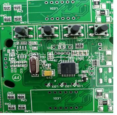
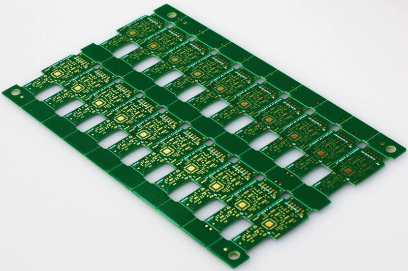
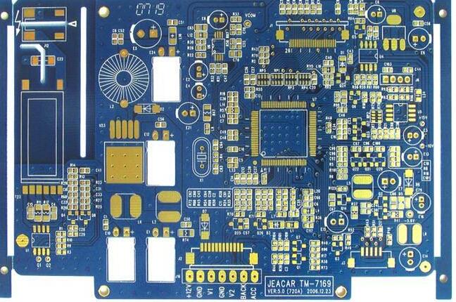
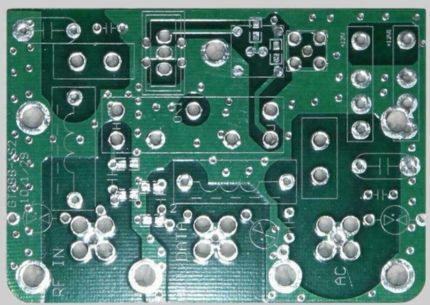
Copper clad laminate (CCL) as a PCB substrate is used as a substrate material in PCB manufacturing. It mainly plays the role of interconnection, insulation and support for the PCB. It has a great impact on the transmission speed, energy loss, and characteristic impedance of the signal in the circuit. Therefore, PCB performance, quality, processability in manufacturing, manufacturing level, manufacturing cost, long-term reliability and stability, etc. depend to a large extent on the material of the copper clad laminate. Next, I will list the top 5 PCB substrates frequently used by circuit board manufacturers.
1. Lead-free compatible copper clad laminate substrate
At the EU meeting on October 11, 2002, two "European Directives" with environmental protection content were passed. They will formally implement the resolution on July 1, 2006. The two "European Directives" refer to the "Electrical and Electronic Product Waste Directive" (referred to as WEEE) and the "Restriction of the Use of Certain Hazardous Substances" (referred to as RoHs). In these two statutory directives, the requirements are clearly mentioned. The use of lead-containing materials is prohibited. Therefore, the best way to respond to these two directives is to develop lead-free copper clad laminates as soon as possible.

2. High performance copper clad laminate
The high-performance copper clad laminates referred to here include low dielectric constant (Dk) copper clad laminates, copper clad laminates for high frequency and high speed PCBs, high heat resistance copper clad laminates, and various substrate materials for multi-layer laminates (resin coated copper Foil, organic resin film that constitutes the insulating layer of laminated multilayer board, glass fiber reinforced or other organic fiber reinforced prepreg, etc.). In the next few years (to 2010), in the development of this type of high-performance copper clad laminates, according to the forecasted future development of electronic installation technology, the corresponding performance index values should be reached.
3. Substrate material for IC package carrier board
The development of substrate materials for IC packaging substrates (also known as IC packaging substrates) is currently a very important topic. It is also an urgent need to develop my country's IC packaging and microelectronics technology. With the development of IC packaging in the direction of high frequency and low power consumption, IC packaging substrates will be improved in important properties such as low dielectric constant, low dielectric loss factor, and high thermal conductivity. An important subject of future research and development is the effective thermal coordination and integration of substrate thermal connection technology-heat dissipation.
Four, copper clad laminates with special functions
The copper clad laminates with special functions referred to here mainly refer to: metal-based (core) copper clad laminates, ceramic-based copper clad laminates, high-dielectric constant laminates, copper clad laminates (or substrate materials) for embedded passive component-type multilayer boards, Copper-clad laminates for optical-electric circuit substrates, etc. The development and production of this type of copper clad laminate is not only required for the development of new technologies for electronic information products, but also for the development of my country's aerospace and military industries.
Five, high-performance flexible copper clad laminate
Since the large-scale industrial production of flexible printed circuit boards(FPC), it has experienced more than 30 years of development. In the 1970s, FPC began to enter the mass production of real industrialization. Development to the late 1980s, due to the advent and application of a new class of polyimide film materials, FPC without adhesive type FPC (generally referred to as "two-layer FPC"). In the 1990s, the world developed a photosensitive cover film corresponding to high-density circuits, which caused a great change in the design of FPC. Due to the development of new application areas, the concept of its product form has undergone a lot of changes, and it has been expanded to include a larger range of substrates for TAB and COB. The high-density FPC that emerged in the second half of the 1990s began to enter large-scale industrial production. Its circuit pattern has rapidly developed to a more subtle level. The market demand for high-density FPC is also growing rapidly.
You know, the production and development of PCB substrates are synchronized with the current electronic technology PCB industry. Therefore, in the era of rapid development of the electronics industry, the update of the substrate version is particularly important.