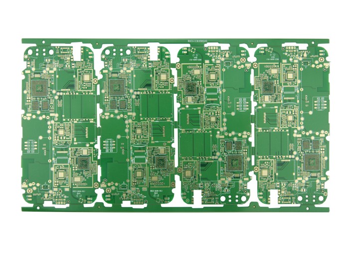
Ways to save PCB manufacturing costs

In order to make the cost of PCB board as low as possible, many factors must be considered:
The size of the board is naturally an important point. The smaller the board, the lower the cost. Part of the PCB size has become the standard, and the cost will naturally decrease as long as the size is adjusted. There is some information about standard sizes on the CustomPCB website.
Using smt will save money than THT, because the parts on the PCB will be denser (and smaller).
On the other hand, if the parts on the board are very dense, then the wiring must be finer, and the equipment used must be relatively higher-level. At the same time, the materials used must be more advanced, and more care must be taken in the design of the wires, so as not to cause power consumption and other problems that will affect the circuit. The cost of these problems can be more than the savings of reducing the size of the PCB.
The more layers, the higher the cost, but PCBs with fewer layers usually increase the size.
Drilling takes time, so the fewer pilot holes, the better.
Buried vias are more expensive than vias through all layers. Because the buried hole must be drilled before joining.
The size of the hole on the board is determined according to the diameter of the part pin. If there are parts with different types of pins on the board, because the machine cannot use the same drill bit to drill all the holes, it is relatively time-consuming, which also means that the manufacturing cost is relatively increased.
Electronic testing using flying probe method is usually more expensive than optical method. Generally speaking, optical testing is sufficient to ensure that there are no errors on the PCB.
decide to use the packaging method, and the size of each PCB
When the technology and the number of circuits used in each PCB are determined, the next step is to determine the size of the board. If the design is too large, then the packaging technology must be changed or re-divided. When choosing a technology, the quality and speed of the circuit diagram must also be considered.
The above is the introduction of P's method of saving PCB manufacturing costs. Ipcb is also provided to PCB manufacturers and PCB manufacturing technology.