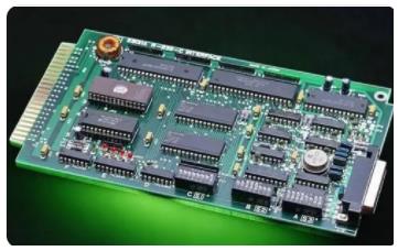
PCB substrates that are becoming more and more environmentally friendly
With the development of electronic equipment in the direction of miniaturization, light weight, multi-function and environmental protection, the printed circuit board as its basis has also developed in these directions accordingly, and the PCB substrate material used for the printed board should naturally be adapted. These needs.
Environmentally friendly materials
Environmentally-friendly products are required for sustainable development, and environmentally-friendly printed boards require environmentally-friendly materials. For the copper clad laminate, the main material of the printed board, the toxic polybrominated biphenyl (PBB) and polybrominated diphenyl ether (PBDE) regulations are prohibited in accordance with the EU RoHs decree, which involves the elimination of bromine-containing flame retardant copper clad laminates Agent. At present, advanced countries in the world have begun to adopt a large number of halogen-free copper clad laminates, while domestic halogen-free copper clad laminate products have only been successfully developed in large foreign-funded enterprises. Many small and medium-sized copper clad laminates are still stuck in the traditional The production of copper clad laminates failed to meet the requirements of environmental protection bans.

In addition to being non-toxic, environmentally-friendly products also require the products to be recycled and reused after being discarded. Therefore, the insulating resin layer of the printed board substrate is considering changing from a thermosetting resin to a thermoplastic resin, which facilitates the recycling of waste printed boards. After heating, the resin is separated from the copper foil or metal parts, and each can be recycled and reused. In this regard, foreign countries have successfully developed high-density interconnect printed boards that have been successfully applied to the build-up method, but there has been no news in China.
Solderable coating materials on the surface of printed boards, the most traditionally used tin-lead alloy solder, now the EU RoHS decree bans lead, and the alternative is tin, silver or nickel/gold plating. Foreign electroplating chemical companies have developed and launched chemical nickel/immersion gold, chemical tin, and chemical silver plating drugs in the past few years, but no domestic suppliers of the same type have launched similar new materials.
Cleaner production materials
Cleaner production is an important means to realize the sustainable development of environmental protection, and to achieve cleaner production requires supplementary cleaner production materials. The traditional printed board production method is the subtraction method of copper foil etching to form patterns, which consumes chemical corrosion solutions and generates a lot of waste water. Foreign countries have been developing and applying non-copper foil catalytic laminate materials, using the additive process of direct electroless copper deposition to form circuit patterns, which can eliminate chemical corrosion and reduce waste water, which is conducive to clean production. The development of this type of laminate material used in the additive process is still blank in China.
The cleaner inkjet printing wire pattern technology that does not require chemical syrup and water cleaning is a dry production process. The key to this technology is inkjet printers and conductive paste materials. Nowadays, nano-scale conductive paste materials have been successfully developed abroad, which enables inkjet printing technology to enter practical applications. This is a revolutionary change for printed boards towards cleaner production. Domestically, there is a lack of micron-level conductive paste materials that meet the use of printed board cross-line and through-holes, and nano-level conductive paste materials are even more shadowless.
In clean production, we also look forward to non-cyanide gold electroplating process materials, chemical copper deposition process materials that do not use harmful formaldehyde as a reducing agent, etc. It is necessary to speed up the development and application of printed board production.
High-performance materials
The digital development of electronic equipment has higher requirements on the performance of the supporting printed circuit boards. At present, there are requirements for low dielectric constant, low moisture absorption, high temperature resistance, high dimensional stability, etc. The key to meeting these requirements is to use high-performance copper clad laminate materials. In addition, in order to achieve lighter, thinner, and higher-density printed boards, thin fiber cloth and thin copper foil copper clad laminate materials are required.
The key to highlighting the light, thin and flexible characteristics of flexible printed boards is flexible copper clad laminate materials. Many digital electronic devices require the application of high-performance flexible copper clad laminate materials. At present, the direction to improve the performance of flexible copper clad laminates is adhesive-free flexible copper clad laminate materials.
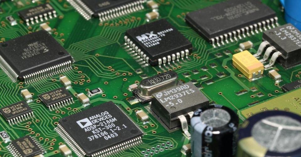
The IC package carrier board is already a branch of the printed board, and is now widely used in new IC packages represented by BGA and CSP. The IC package carrier uses a thin organic substrate material with good high frequency performance, high heat resistance and high dimensional stability. High-performance materials have been applied abroad, and further improvements are being made and new materials are being produced. In contrast, domestic counterparts are still in a blank in many high-performance materials.
In order to make China a big and powerful country in the printed circuit industry, there is an urgent need for materials for printed circuit boards made in China.
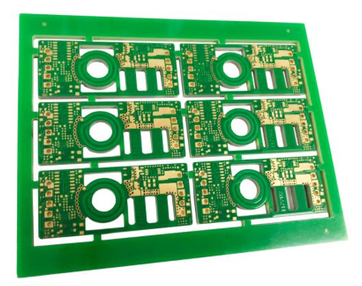
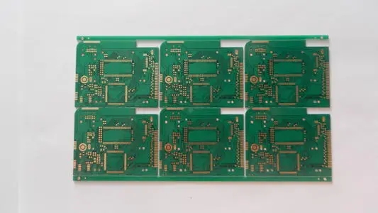
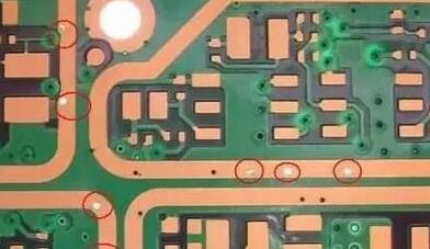
Printed circuit board material classification
There are many types of printed circuit board materials used in SMT processing, which can be divided into main materials and auxiliary materials according to their applications.
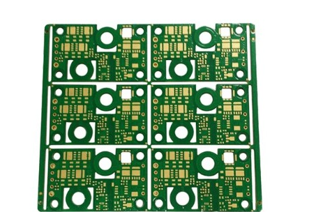
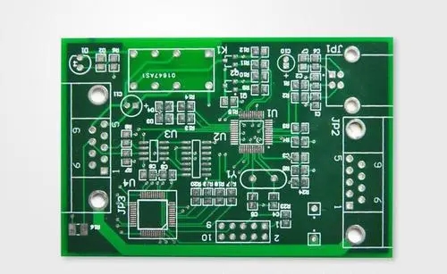
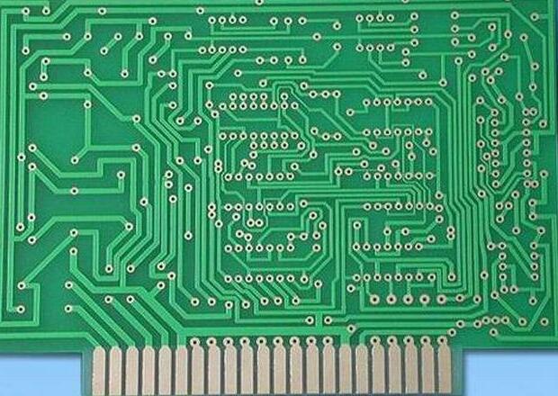
Main materials: raw materials that become part of the product, such as copper clad laminates, solder resist inks, marking inks, etc., also known as physical and chemical materials.
Auxiliary materials: materials consumed in the production process, such as photoresist dry film, etching solution, electroplating solution, chemical cleaning agent, drilling pad, etc., also known as non-physical materials.