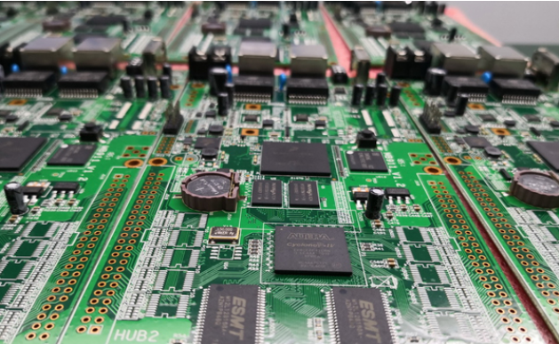
Here we focus on the production technology of single-sided printed circuits. The layout of the components on the printed PCB board is essentially the layout of the printed circuit. The general principles are:

1. Under normal conditions, all components should be arranged on one side of the printed circuit board, and the side with the model, specification and nameplate printed on the components should face up to facilitate inspection, processing, installation and maintenance. . For single-sided printed board components, they can only be installed on the side where there is no printed circuit copper foil. If insulation is required, an insulating film can be used between the components and the printed circuit (photographic negatives can be used as a substitute), or a gap of 1" 2mm can be left between the components and the printed circuit.
2. The components on the board should be arranged in a straight line according to the order of the circuit schematic diagram as much as possible, and the circuit arrangement should be compact, dense and tidy. The wiring at all levels should not be parallel. This is particularly important for high-frequency and broadband circuits.
3. If all electronic components cannot be installed on a printed board due to the limitation of the board, or the whole machine must be divided into several printed boards for shielding purposes, then each piece should be assembled. The printed circuit constitutes an independent function for individual adjustment, overhaul and maintenance.
4. In order to reduce the size or improve the mechanical strength, one or more pieces can be installed in addition to the main printed board: auxiliary bottom board. The auxiliary bottom board can be metal, printed board or insulating board. Some bulky components, such as transformers, chokes, large capacitors, relays, etc., are installed on the auxiliary board, and accessories are used to fasten it.
5. For components with strong electromagnetic radiation and sensitive components with electromagnetic induction, the installation position should avoid mutual influence between them. The distance between them can be increased or shielded. The direction in which the components are placed should cross the adjacent printed wires. Especially for inductive devices, special attention should be paid to measures to prevent electromagnetic interference.
6. The heating components should be arranged in positions that are conducive to heat dissipation. When necessary, a separate heat sink can be provided to reduce the temperature and reduce the impact on neighboring components. The radiator of the transistor and the rectifier component can be directly installed on its shell, or the radiator can be fixed on the printed circuit board, the casing or the bottom plate of the machine. For high-power resistors, you can use a 1"3mm thick aluminum curved surface cylinder with good thermal conductivity, which is tightly attached to the housing of the resistor and fixed to facilitate heat dissipation.
7. For heat-sensitive components, stay away from high-temperature areas, or use an isolation wall structure to disconnect the heat source to avoid the influence of heating components.
8. Heavy and large components should be placed as close to the fixed end of the printed board as possible, and the center of gravity should be lowered to improve the mechanical strength, vibration resistance and impact resistance, and reduce the load deformation of the printed board.
9. General components can be directly soldered on the printed circuit board. However, when the component exceeds 15g or the volume exceeds 27cm3, additional metal fasteners should be considered to improve the vibration and impact resistance.
10. Under the premise of ensuring electrical performance, the components should be arranged in parallel or perpendicular to each other for orderliness and beauty. Under normal circumstances, it is not allowed to overlap components. If it is necessary to reduce the size of the plane, the components must be fixed with mechanical support.
11. The ground wire (common wire) generally cannot be made into a closed loop. Refer to Figure 5-1 (a) for the correct method to prevent the circuit from self-excitation.
12. Some components such as integrated circuits with high power consumption, large or medium power transistors, resistors, etc. should be arranged in places where heat is easy to dissipate, and separated from other components by a certain distance.
13. Components that need to be connected to external circuits through printed connectors, especially integrated circuit blocks that generate large current signals or important pulses, should be placed on the board as close to the plug as possible.
14. For signal source circuits such as clock pulse generators and timing pulse generators, ample installation positions should be considered in the layout to reduce and avoid interference to other circuits.
15. For the electronic circuit mounted on the vibration device, the axial direction of the components on the printed circuit board should be consistent with the main vibration direction of the machine.
16 In order to improve the reliability of the device, it is necessary to minimize the contact points between the printed plug-in unit and the socket used in the entire device, the connection line of the bottom plate and the solder joints. When you can use a larger printed circuit board to solve the problem, do not divide it into two or more small pieces.
The method to determine the size of the printed board is to first arrange the integrated blocks and other components that are determined to be installed on a printed board on a piece of paper according to the layout requirements. When arranging, it is necessary to adjust at any time to make the aspect ratio of the printed board meet or approach the actual requirement. There should be a certain gap between each component, generally 5"15mm, and the circuit with special requirements should also be widened. If the gap is too small, the components are not easy to dissipate, and it is inconvenient to debug and repair; if the gap is too large, the size of the printed board will be large., The interference caused by the printed wire resistance, distributed capacitance and inductance will also increase. After all the components are placed, the approximate size of the printed board will be known. For example, the aspect ratio of the printed board formed is in accordance with the actual requirements. In and out, the length and width warp can be adjusted appropriately without destroying the layout.
The above is the introduction of the layout of the components on the printed circuit board. Ipcb is also provided to PCB manufacturers and PCB manufacturing technology.