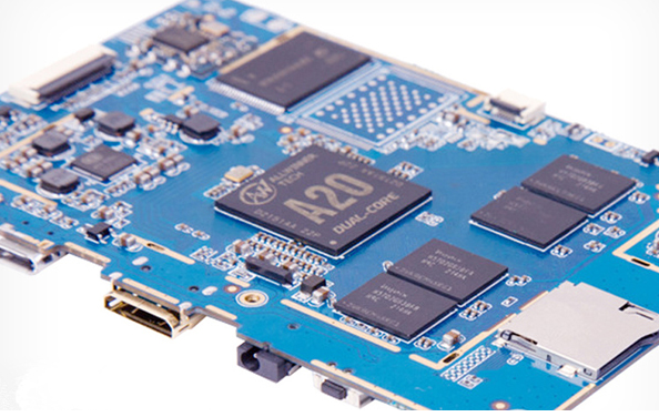
Shield (shield cover/case/bracket) is an alloy metal cover, which is a vital component to reduce the radiation of the display. The inside of the display contains components such as electron guns, high-voltage packages and PCB boards. They emit high-intensity electromagnetic radiation during work. The shielding cover can play a shielding role, blocking the absolutely part of the electromagnetic wave in the cover, thereby protecting the user from The harm of electromagnetic radiation, while avoiding interference with other electrical appliances around it, to a certain extent, it also ensures that the components are protected from dust and prolongs the service life of the display. It is mainly used in mobile phones, GPS and other fields.

Shielding is the isolation of metal between two spatial areas to control the induction and radiation of electric fields, magnetic fields and electromagnetic waves from one area to another. Specifically, shielding is used to surround the interference sources of components, circuits, assemblies, cables or the entire system to prevent the interference electromagnetic field from spreading; shielding to surround the receiving circuit, equipment or system to prevent them from being exposed to the outside world The influence of electromagnetic fields. Because the shielding body absorbs energy (eddy current loss), reflected energy (reflection of electromagnetic waves on the interface of the shielding body) and offsetting energy (electrical Magnetic induction produces a reverse electromagnetic field on the shielding layer, which can offset part of the interference electromagnetic wave), so the shield has the function of reducing interference.
(1) When the frequency of the interfering electromagnetic field is high, the eddy current generated in the low-resistivity metal material is used to form the cancellation effect of the external electromagnetic wave, so as to achieve the shielding effect.
(2) When the frequency of interfering electromagnetic waves is low, materials with high magnetic permeability should be used, so that the lines of magnetic force are limited to the inside of the shield and prevent spreading to the shielded space.
(3) In some cases, if a good shielding effect is required for both high-frequency and low-frequency electromagnetic fields, different metal materials are often used to form a multi-layer shielding body.
1. The lid material can be ZSNH zinc-tin-nickel alloy (cheap), nickel silver (good performance and easy processing), or stainless steel (no tin can only be used for the lid). The bracket material is ZSNH zinc-tin-nickel alloy or nickel silver to ensure good welding performance. But now there are customers who use ZSNH for both the upper and lower covers.
2. ZSNH zinc-tin-nickel alloy base has a thickness of 0.2mm and a cover of 0.13mm. Stainless steel cover plate 0.13mm nickel silver base thickness 0.2mm, cover 0.13mm, single-piece, two-piece type, material: nickel silver, stainless steel, ZSNH zinc-tin-nickel alloy
3. The gap between the cover and the bracket is 0.05mm, the z-direction gap is 0mm, and the distance between the components is more than 0.4mm
4. After flattening, leave the width of the punching area 0.5mm.
5. The width of the shielding cover pad is between 0.7mm~1mm, too small is not conducive to the patch, and too large is easy to be interfered by the outside world. The minimum gap between the shielding cover and the bottom of the shielding cover is 0.5mm (the minimum distance between the bracket pad and the pad is 0.3mm).
6. The height of the float tin is 0.1mm when the bracket is smt, and the flatness of the cover is 0.1mm. After the shielding cover is assembled, the gap between the upper device or the shell should be at least 0.2mm
7. A suction cup area with a diameter of 5mm should be pre-designed at the center of gravity of the shielding bracket.
8. There should be one or two through holes with a diameter of 0.7~1mm on each side of the surrounding wall of the shielding bracket for clamping the shielding cover. The card hole should not be too many, otherwise it is difficult to disassemble and can be made by the supplier. We will give the position and size.
9. The bottom surface of the wall around the shielding cover should be 0.5mm away from the PCB to prevent the shielding bracket from over-eating tin to withstand the shielding cover.
10. The diameter of the heat dissipation hole of the shield cover is 1mm.
11. If the shielding cover or shielding bracket has a flat drop, pay attention to the side cut through the drop boundary, otherwise it cannot be processed. In addition, a hole with a diameter of 3mm should be punched at the corner of the drop in the plane, otherwise it will tear.
12. If the shielding cover or shielding bracket has a plane drop, pay attention to the drop angle of 35~40 degrees, and it will break when processing a too large angle.
13. If the shielding cover or shielding bracket has a plane drop, the clearance between the bracket and the cover surface at the drop is not 0, and should be 0.1mm.
14. The distance between the plane cut-out of the shielding bracket and the outer wall of the side wall should be more than 1mm. If there is a downward bend inside, the side wall of the bend is 0.5mm away from the outer wall. At this time, the plane is directly attached to the side wall and cut.
15. The corner R0.5mm in the cut-out area of the shielding bracket.
16. The shielding bracket and the PCB are not welded on the whole surface, but the Great Wall pin welding of 2-1-2-1mm method should be used, with 2mm contact and 1mm hanging in the air to facilitate tin climbing. In this way, the attachment strength of the shielding cover can be increased.
17.1. It is matched with SHIELDING-BOX.
2. The surface flatness is within 0.1MM.
3. The inner corner of the bending is R0.1MM, and the unfilled corner is R0.1MM.
4. The bending angle is 90°±0.5.
5. Unmarked tolerances are in accordance with the tolerance level shown in the figure
6. The dimensions with "*" in the figure are QC controlled dimensions.
7. Please review with the engineer before opening the mold. (Tolerance size: the size less than 20mm is controlled within +-0.05mm; the size greater than 20mm is controlled within +-0.1mm; the flatness of the top layer is controlled within +-0.1mm;)
The above is the introduction of smart phone PCB design-shielding cover, Ipcb also provides PCB manufacturers and PCB manufacturing technology