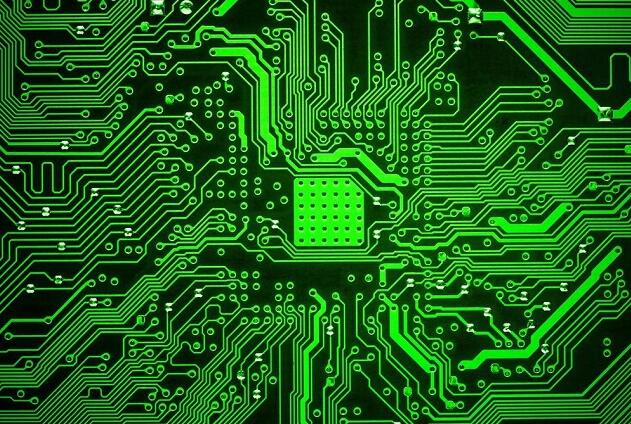
In the process of PCB design and production, engineers not only need to prevent PCB in the manufacturing process of accidents, but also need to avoid design mistakes.
This paper summarizes and analyzes several common PCB problems, hoping to bring some help to your design and production work.

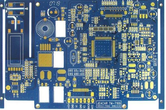
Fault 1: The PCB is short-circuited
This problem is one of the common failures that will directly cause the PCB board to fail to work. There are many reasons for this problem, and we will analyze them one by one.
PCB short circuit is caused by improper design of welding pad. At this time, round welding pad can be changed to oval shape to increase the distance between points to prevent short circuit.
Improper design of PCB parts will also cause short circuit of the board and fail to work. If the SOIC foot is parallel to the tin wave, it is easy to cause a short circuit accident. At this time, the direction of the parts can be appropriately modified to make it vertical with the tin wave.
Another possibility that can cause PCB short circuit failure is the automatic plug-in pin. As IPC stipulates that the length of the pin shall be less than 2mm and the parts may be dropped if the Angle of the pin is too large, so it is easy to cause short circuit, so the solder joint shall be more than 2mm away from the line.
In addition to the three reasons mentioned above, there are some reasons can lead to the fault of PCB board, such as substrate hole is too big, tin stove temperature is too low, board face poor solderability and resistance welding membrane failure, surface pollution, etc., are relatively common fault reason, engineers can contrast the above reasons and failure to eliminate and check them one by one.
Problem two: dark and granular contacts appear on PCB board
The problem of dark or granular contact on PCB board is mostly due to the contamination of solder and too much oxide mixed in the dissolved tin, forming the structure of solder spot is too brittle. Care must be taken not to be confused with the dark color caused by using low tin content solder.
Another reason for this problem is that the solder itself used in the process of manufacturing changes, too much impurity content, need to add pure tin or replace the solder. Physical changes of speckled glass fiber deposition, such as separation between layers. But this situation is not bad solder joints. The reason is that the substrate is heated too high, need to reduce the preheating and soldering temperature or increase the substrate speed.
Problem three: PCB solder spot becomes golden yellow
In general, the solder on PCB board is silver gray, but occasionally there are golden solder spots. The main reason for this problem is that the temperature is too high. In this case, you only need to lower the temperature of the tin furnace.
Problem four: board of undesirable also suffer environmental influence
Due to the structure of PCB itself, it is easy to cause damage to PCB board under adverse environment. Extreme temp
erature or temperature variation, excessive humidity, high intensity vibration and other conditions are leading to the performance of the board reduced or even scrapped factors. For example, a change in ambient temperature can cause the board to deform. This will damage the solder joints, bend the plate shape, or may cause the copper trace on the plate to break.
Moisture in the air, on the other hand, can cause oxidation, corrosion and rust on metal surfaces such as exposed copper traces, solder joints, pads and component leads. Accumulation of dirt, dust, or debris on the surface of components and boards can also reduce air flow and cooling of components, leading to overheating and performance degradation of the PCB. Vibration, dropping, hitting, or bending the PCB can deform it and cause cracks, while high currents or overvoltages can cause the PCB to be punctured or lead to rapid aging of components and paths.
Problem five: PCB open circuit
Open circuit occurs when the trace breaks, or when solder is only on the pad and not on the component lead. In this case, there is no adhesion or connection between the component and the PCB. Just like short circuits, these can occur during production or welding and other operations. Vibration or stretching of circuit boards, dropping them, or other mechanical deformations can destroy traces or solder joints. Similarly, chemical or moisture can cause solder or metal parts to wear, which can cause component leads to break.
Problem six: loose or misplaced components
During reflow welding, small parts may float on the molten solder and eventually detach from the target solder spot. Possible causes of displacement or tilt include vibration or bounce of components on welded PCB boards due to insufficient board support, reflow furnace setup, solder paste problems, human error, etc.
Problem seven: welding problem
The following are some problems caused by poor welding practices:
Disturbed solder joint: The solder moves before solidification due to external disturbance. This is similar to the cold solder spot, but for a different reason, and can be corrected by reheating and ensuring that the solder spot is protected from external interference while it cools.
Cold welding: This occurs when the solder does not melt properly, resulting in rough surfaces and unreliable joints. Cold spots may also occur because excess solder prevents complete melting. The remedy is to reheat the joint and remove excess solder.
Solder bridge: This occurs when solder is crossed and two leads are physically joined together. These have the potential to form unexpected connections and short circuits, which can cause the component to burn or burn off the wiring if the current is too high.
Pad: Insufficient wetting of pins or leads. Too much or too little solder. A pad that has been raised by overheating or rough welding.
Problem 8: Human error
Defects in PCB manufacturing are largely the result of human error, with faulty manufacturing processes, misplacement of components, and poor manufacturing practices accounting for up to 64% of avoidable defects in most cases. The likelihood of defects increases with circuit complexity and number of manufacturing processes due to: densely packed components; Multiple circuit layer; Fine wiring; Surface welding assembly; Power supply and ground.
Although every manufacturer or assembler wants to produce a PCB that is defect-free, there are several design and manufacturing process challenges that cause PCB problems.
Typical problems and results include the following points: poor welding will lead to short circuit, open circuit, cold welding point and so on; The dislocation of the plate will lead to poor contact and poor overall performance; Poor insulation of copper trace leads to arc between trace lines. The copper trace line and the path between too close, it is easy to appear the risk of short circuit; Insufficient thickness of the circuit board can lead to bending and fracture.