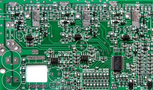
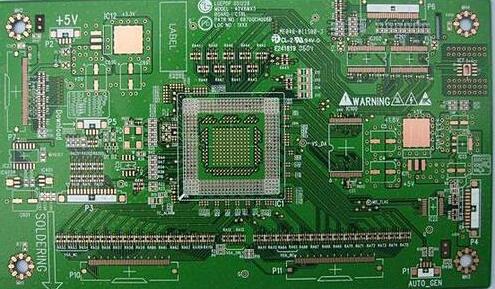
Any layer through hole technology characteristics
ALIVH has an advantage over HDI in that it can drill holes between layers in a way that HDI cannot.Generally, domestic manufacturers achieve complex structure, that is, the design limit of HDI is third-order HDI PCB board. Because HDI does not completely use laser drilling, the embedded holes in the inner layer are mechanical holes, so the requirements of the hole plate are much larger than the laser holes, and the mechanical holes have to occupy the space on the level through. Therefore, generally speaking, there is a big gap between the HDI structure and ALIVH technology's arbitrary
drilling, and the pore size of the inner core plate can also be used as 0.2mm microhole. So the wiring space of ALIVH board is probably much better than that of HDI. ALIVH is also more costly and difficult to process than HDI.

Embedded resistance, capacity and embedded components
High-speed access to the Internet and social networks requires high integration and miniaturization of handheld devices. It currently relies on 4-N-4 HDI technology. But for the next generation of new technologies to achieve higher interconnect density, in this area, embedding passive and even active components into PCBS and substrates can meet these requirements. When designing consumer electronics such as mobile phones and digital cameras, it is a current design choice to consider how to embed passive and active components into PCBS and substrates. This approach may vary slightly depending on the vendor you use. Another benefit of embedding parts is that the technology provides protection against intellectual property and prevents so-called reverse design. Allegro PCB Editor offers industrial grade solutions. Allegro PCB Editor also works closely with HDI boards, adagio and embedded parts. You can get the right parameters and constraints to complete the embedded part design. The embedded device design can not only simplify the SMT process, but also greatly improve the cleanliness of the product.
Buried resistance, buried capacity design
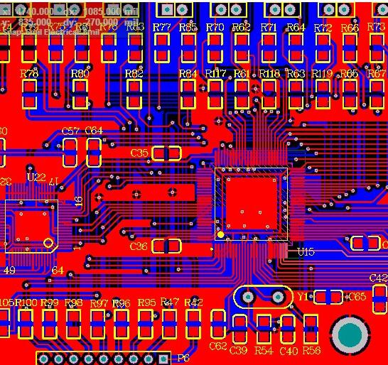
Buried resistance, also known as buried resistance or film resistance, is the special resistance material pressed on the insulating substrate, and then through printing, etching and other processes, to obtain the required resistance value, and then pressed together with other PCB board layer, forming a plane resistance layer. Common PTFE embedded resistance multilayer PCB manufacturing technology, can achieve the required resistance.
Buried capacitance is to use materials with high capacitance density and reduce the distance between layers to form a large enough inter-plate capacitance to play a role of decoupling and filtering of the power supply system, thus reducing the discrete capacitance required on the board and achieving better high-frequency filtering characteristics. Because the parasitic inductance is very small, the resonant frequency points will be better than normal or low ESL capacitors.
Due to the maturity of technology and technology, as well as the need of high-speed design for power supply system, the application of buried capacity technology is more and more, the use of buried capacity technology, we first have to calculate the size of plate capacitance FIG. 6 plate capacitance calculation formula
Among them:
C is the capacitance of buried capacity (plate capacitance)
A is the area of the plates. In most designs, it is difficult to increase the area between the plates when the structure is determined
D_k is the dielectric constant of the medium between plates, and the capacitance between plates is proportional to the dielectric constant
K is the Vacuum permittivity, also known as the Vacuum permittivity, which is a physical constant with a value of 8.854 187 818* 10-12 farad /m (F/m);
H is the thickness between planes, and the capacitance between plates is inversely proportional to the thickness, so we need to reduce the thickness between layers to obtain a larger capacitance. 3M C-PLY buried material can achieve the thickness of 0.56mil between layers, plus the dielectric constant of 16, which greatly increases the capacitance between plates.
It was calculated that 3M's C-PLY buried material achieved an inter-plate capacitance of 6.42nF per square inch of surface area.
At the same time, the PI simulation tool is also needed to simulate the PDN target impedance, so as to determine the capacitor design scheme of the board, avoiding redundant design of buried capacity and discrete capacitance. Figure 7 is the PI simulation result of a buried capacity design, which only considers the effect of inter-plate capacitance without adding the effect of discrete capacitance.It can be seen that only by increasing the buried capacity, the performance of the entire power supply impedance curve is greatly improved, especially above 500MHZ, which is the frequency band where the board stage discrete filter capacitor is difficult to play a role, and the plate capacitor can effectively reduce the power supply impedance.