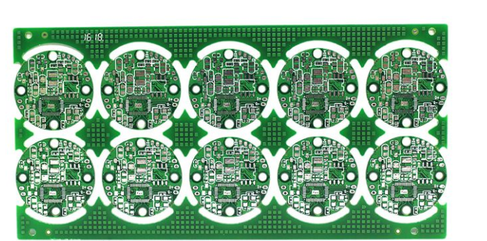
In the process of manufacturing PCBA flip-chip bumps, after introducing an insulating layer to flatten the topological map of the flip-chip IC surface, the contract manufacturer can use uniform design rules to process ICs with different surface topologies. For (China) packaging design companies, understanding the causes and solutions of this technology is helpful to grasp the latest technological trends in this field.
More than 30 years ago, IBM first introduced the flip-chip interconnect structure to the manufacturing industry. The company not only introduced the concept of three-dimensional (3D) interconnection structure, but also took the lead in proposing all the technologies and design rules for assembling bare-chip PCBA into modules or PCBA assembling the backplane. Since then, some larger manufacturing companies have also begun to build flip-chip production lines. They either obtained licenses directly from IBM (such as Motorola, AMD, etc.), or improved the PCBA assembly process of large companies like Delco. For large companies, the entire process from wafer processing to finished product delivery can be fully controlled. Therefore, it is entirely possible to combine process rules with wiring software and adopt a smart design process. However, the situation is different now. Contract manufacturing is limited by the flip chip processing process and faces some problems that have not been encountered in the past.

The manufacturing processes and design rules adopted by IC manufacturers are very different, making it difficult for contract manufacturers who manufacture flip-chip bumps to choose which automatic wiring software to perform flip-chip I/O layout and metal interconnection. For this reason, it is necessary to introduce an insulating layer to planarize the topological map of the flip-chip IC surface, so that contract manufacturers can use uniform design rules to deal with ICs with different surface topologies.
Contract manufacturing chain
The manufacturing industry has long changed the previous model of large-scale, vertically integrated structures. Today, for global manufacturers who design and process flip-chip chips, the manufacturing process can basically be broken down into three stages (Figure 1). First, design and produce chips. In most cases, design and production may be carried out separately; second, design and manufacture flip-chip interconnect structures; third, design substrates or backplanes, and adhere the chips to the circuit board. Contract manufacturers are in the second stage of the manufacturing chain.
The manufacturing process can basically be divided into three stages-PCBA processing and assembly for the surface smoothing process for the production of flip chip bumps
First, design and produce chips. In most cases, design and production may be separated; second, design and manufacture flip-chip interconnect structures; third, design substrates or bottom plates, and adhere the chips to the product middle.
For manufacturers who can control the entire process, they can seamlessly integrate their chip designs into flip-chip interconnect packages. However, the contract manufacturer cannot control the entire process of wafer design and manufacturing, so it is necessary to add an additional wiring layer to convert the uneven wiring structure of the wafer into a planar array interconnect structure. This additional wiring layer is usually called metal or I /O
The secondary PCBA wiring layer, or just called the secondary wiring layer.
Generally speaking, the secondary wiring layer is a thin-film wiring layer composed of aluminum or copper wires, where the wiring can be used as signal wires, power wires and ground wires. The additional layers present in these wirings may require bonding or increase the electronic drift resistance of the current transmission line. At present, this kind of thin-film wiring layer is generally manufactured in the back-end processing. Therefore, according to specific design requirements, its thickness is usually between 1 and 3 μm, and the width is usually between 12 and 100 μm.
Regardless of whether the secondary wiring of the flip chip I/O is performed, a solder interconnection structure must be formed on the I/O bonding pad. In the process of soldering interconnect structure processing, PCBA assembly and rework, a metal compound layer will appear. The most reliable UBM structure requires the thinnest possible support structure. In the process of processing and PCBA assembly, a high-lead solder joint based on a common metal can restrict the formation of fragile metal compound layers. Figure 2 shows a thin-film UBM welding interconnection structure. There are monographs on the relationship between the thickness of the metal compound layer and the thermal cycle period for reference.
A thin-film UBM welding interconnection structure-PCBA processing and assembling a surface smoothing process for the production of flip chip bumps
The problems faced by contract wafer suppliers come from two aspects. On the one hand, they are unable to control the process flow, and on the other hand, they lack an understanding of the chip topology. Many manufacturers require fabs to provide flip chip bumping services. At the same time, in order to control costs or protect the safety of their manufacturing chain, they usually choose other foundries to manufacture chips with exactly the same functions.
Conclusion of this article
At present, the main difficulties faced by flip chip interconnection design are in two aspects: 1. Metal interconnection process that meets all electrical parameters required by die and substrate; 2. Three-dimensional geometric structure that meets all PCBA assembly and processing processes . Suppliers that provide contract bump processing services are facing a series of problems that seem to be difficult to overcome. In order to combine automatic wiring tools with flip chip bump processing and secondary wiring processes, it is necessary to master the processing control process. It is almost impossible for contract manufacturers of wafers to obtain more metal layer information. Wafer-bumping houses may be able to solve this problem, just as people have used packaging to solve IC manufacturing process defects. In addition, in fact, in addition to mastering the precise design dimensions of the top layer, more information may be difficult to obtain.
In order to solve the above problems, it is necessary to use a uniform planar insulating layer in the manufacturing process, such as the BCB material manufactured by Dow Chemical Company. Covering the organic passivation insulating layer may increase the cost, but it does require a flat surface to process the interconnect structure to achieve highly reliable PCBA assembly.