PCB circuit board original composition structure
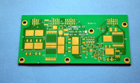
PCB circuit board is divided into route map surface, dielectric layer, hole, solder mask printing ink, silk screen ink, metal surface treatment, etc. in the original structure.
1. Route and cad map (Pattern): The route is a special tool for connecting and disconnecting the originals. In the design, a large copper surface will be designed as a grounding device and a power layer. The route and the cad drawing are made at the same time.
2, Dielectric layer (Dielectric): Used to maintain the insulation between the routes and the layers, aliased as plate.
3. Hole (Throughhole/via): Buried guide holes can connect and disconnect the routes above two levels. Larger buried guide holes are used as part plug-ins. In addition, there are non-buried holes (nPTH) generally used as surface layers. SMD positioning, used to fix screws when assembling.
4. Solderresistant/SolderMask: Not all copper surfaces need to be tin-on parts, so in areas that do not eat tin, a layer of chemical substances (usually epoxy resins) that block the copper surface from eating tin will be printed ), to prevent short-circuit failures between non-tin-eating routes. According to different processing technology, it is divided into green oil, red oil and blue oil.

5. Silkscreen ink (Legend/Marking/Silkscreen): This is an unnecessary composition. The specific function is to mark the name and position frame of each part on the circuit board, which is convenient for maintenance and identification after assembly.
6. Metal surface treatment (SurfaceFinish): Because the copper surface is very easy to be oxidized in the air in the normal environment, it can not be tinned (the solderability is poor), so maintenance will be carried out on the copper surface that needs to be tinned. Maintenance methods include HASL, ENIG, ImmersionSilver, ImmersionTIn, and organic chemical soldering flux (OSP), all of which have advantages and disadvantages, and are commonly referred to as metal surface treatment. .
Attention points in the design concept of PCB circuit board
In the design concept of PCB circuit boards, attention should be paid to the design concept environment, design concept specifications, design concept specifications and other key points.
According to the already clear circuit board plane specifications and various mechanical positioning, the PCB board surface is produced in the PCB design environment, and the required connectors, buttons/switches, digital display tubes, display lights, input and output are placed according to the positioning regulations., Screw holes, mounting holes, etc., and comprehensively consider and clarify the wiring area and non-wiring area (such as how much area around the screw hole belongs to the non-wiring area. You must pay great attention to the placement of electronic devices. The actual size (occupied area and height), relative position between electronic devices-space specifications, device placement surface, in order to ensure the electrical performance of the circuit board and the feasibility and convenience of production and installation, while ensuring the above Under the condition that the principles can be embodied, the placement of the components should be appropriately modified to make them neat and beautiful. For example, the same components should be placed neatly and in the same direction, and should not be placed in a "scattered" manner.