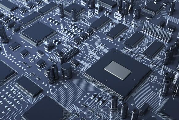
The meaning of BGA in PCBA processing
Pay attention to product innovation in terms of energy saving and emission reduction. PCB factoriesmust learn to attach importance to Internet technology and realize the practical application of automated monitoring and intelligent management in production through the integration of overall industry knowledge.
2. Pay attention to the trend of environmental protection informatization and the development of various environmental protection technologies. PCB factories can start with big data to monitor the company's pollution discharge and treatment results, and find and solve environmental pollution problems in a timely manner. Keep up with the production concept of the new era, continuously improve resource utilization, and realize green production. Efforts to enable the PCB factory industry to achieve an efficient, economical and environmentally friendly production model, and actively respond to the country's environmental protection policy.
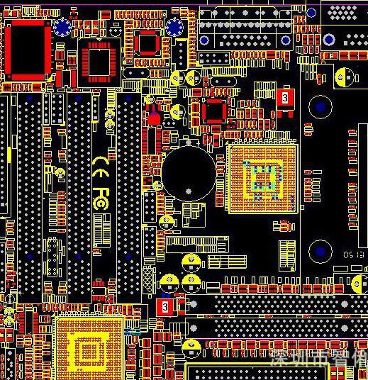
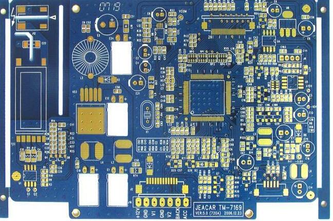
The full name of BGA in PCBA processing is Ball Grid Array (PCB with ball grid array structure), which is a packaging method for integrated circuits using organic substrates. It has: less packaging area; increased functions and increased number of pins; self-centering when the PCB board is melted and easy to tin; high reliability; good electrical performance and low overall cost. PCB boards with BGA generally have many small holes. Most customers' BGA vias are designed with a finished hole diameter of 8-12mil. The distance between the surface of the BGA and the hole is 31.5mil as an example, generally not less than 10.5mil. BGA via holes need to be plugged, BGA pads are not allowed to be filled with ink, and BGA pads are not drilled.

The assembly of BGA devices in PCBA processing is a basic physical connection process. In order to be able to determine and control the quality of such a process, it is required to understand and test the physical factors that affect its long-term reliability, such as the amount of solder, the positioning of wires and pads, and wettability, otherwise it is attempted to be based solely on electronics The results of the test are modified, which is worrying. The performance and assembly of BGA devices are superior to conventional components, but many manufacturers are still unwilling to invest in the ability to develop mass production of BGA devices. The main reason is that it is very difficult to test the solder joints of BGA devices, and it is not easy to guarantee its quality and reliability.
InPCBA processing, BGA devices can consistently achieve a defect rate of less than 20 (PPM) when using conventional SMT process procedures and equipment for assembly and production. Since the beginning of the 1990s, SMT technology has entered a mature stage. However, with the rapid development of electronic products in the direction of convenient/miniaturization, networking and multimedia, higher requirements have been put forward for electronic assembly technology. Density assembly technologies continue to emerge, among which BGA (Ball Grid Array package) is a high-density assembly technology that has entered the practical stage. Our factory is located in China. For decades, Shenzhen has been known as the world's electronics R&D and manufacturing center. Our factory and website are approved by the Chinese government, so you can skip the middleman and buy products on our website with confidence. Because we are a direct factory, this is the reason why 100% of our old customers continue to purchase on iPCB.