Basic steps of PCB design
The basic design process of the circuit board can be divided into the following four steps:

(1) Design of circuit schematic diagram
The design of the circuit schematic diagram mainly uses the schematic editor such as Orcad, ALTIUM DESIGNER to draw the schematic diagram.
(2) Generate network reports
The network report is a report showing the link relationship between the circuit principle and the various components in the circuit. It is the bridge and link between the circuit schematic design and the circuit board design (PCB design). Through the network report of the circuit schematic, you can quickly find the element. The connection between the devices provides convenience for the subsequent PCB design.
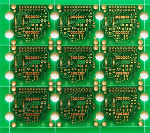
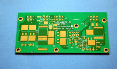
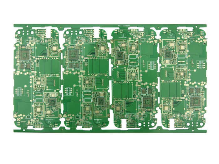
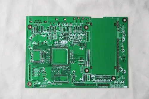
(3) Design of printed circuit board
The design of the printed circuit board is what we usually call the PCB design. It is the final form that the circuit schematic is transformed into. The related design of this part is more difficult than the design of the circuit schematic. We can use Protel DXP, Pads, Design tools such as Allegro to complete this part of the design.
(4) Generate printed PCB board reports
After the printed circuit board design is completed, various reports need to be generated, such as a pin report, a circuit board information report, a network status report, etc., and finally a printed circuit diagram is printed.