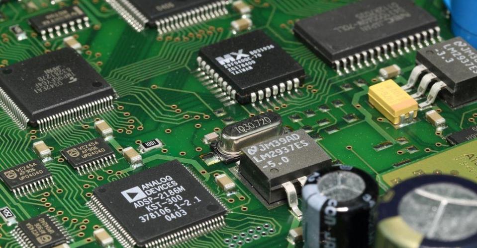
Nowadays, the factors considered in PCB design are becoming more and more complex, such as clock, crosstalk, impedance, detection, manufacturing process, etc., which often makes designers repeat a lot of work such as layout, verification, and maintenance. The parameter constraint editor can compile these parameters into formulas, helping designers better deal with these parameters that sometimes even oppose each other during the design and production process.

In recent years, the requirements for PCB layout and wiring have become more and more complex. The number of transistors in integrated circuits is still rising at the speed predicted by Moore’s Law, which makes the device faster and the rise time of each pulse edge is shortened, and the number of pins is also increasing. More and more-often 500 to 2,000 pins. All of this will bring density, clock, and crosstalk issues when designing the PCB board.
A few years ago, there were only a few "critical" nodes (net) on most PCBs, which usually meant that they were subject to some constraints in terms of impedance, length, and gap. PCB designers generally first manually route these traces, And then use software to make large-scale automatic wiring of the entire circuit. Today's PCBs often have 5,000 or more nodes, and more than 50% of them are critical nodes. Due to the time-to-market pressure, manual wiring is no longer possible at this time. In addition, not only the number of critical nodes has increased, but the constraints of each node have also increased.
These constraints are mainly caused by the correlation of parameters and the increasing complexity of design requirements. For example, the distance between two traces may depend on a function related to node voltage and circuit board material. The rise time of digital IC is reduced. Both high clock speed and low clock speed design will have an impact. Because the pulse is generated faster, the setup and hold time is shorter. In addition, the interconnection delay is an important part of the total delay of high-speed circuit design and is also very important for low-speed design, etc. Wait.
If the circuit board can be designed larger, some of the above problems will be easier to solve, but the current development trend is just the opposite. Due to the requirements for interconnection delay and high-density packaging, circuit boards are becoming smaller, resulting in high-density circuit designs, and at the same time, miniaturization design rules must be followed. The reduced rise time and these miniaturized design rules have made the crosstalk noise problem more and more prominent, and the ball grid array and other high-density packages will also aggravate crosstalk, switching noise, and ground bounce.