If you haven't learned PCB Layout, you will start from scratch with me. A simple question, where do I start? The question is simple, but the answer is more complicated.
First of all, we must understand some basic knowledge, commonly used software: Allegro, Pads, Protel, Orcad, etc. (for the introduction of each software, please refer to related materials).

Before starting PCB Layout, it is necessary to have a sufficient understanding of PCB board.
PCB board, specifications, current technological level.
PCB device information, such as package and related dimensions.
The placement and connection of PCB components, such as how to place some special components.
PCB wiring rules and markings.
To put it bluntly, which devices are used, how to wire, and what kind of motherboard is placed on.
The following is a detailed description:
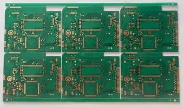
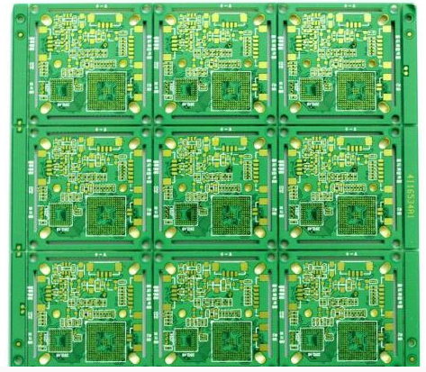
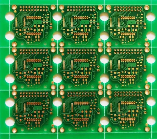
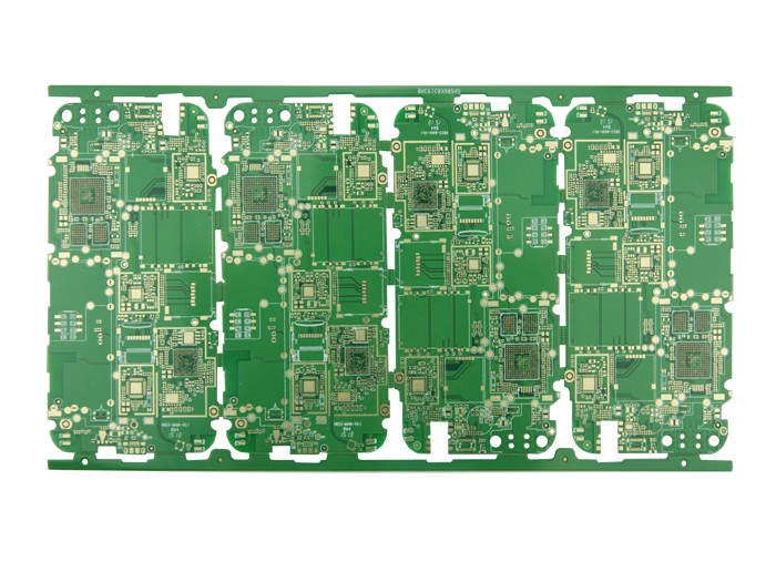
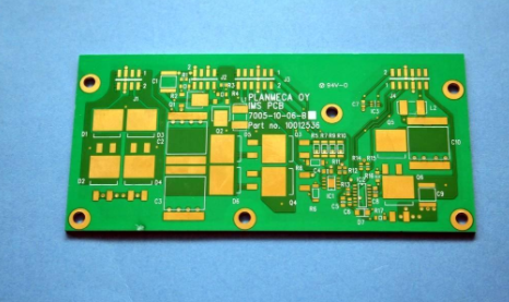
1. PCB board
Common substrate plates include: FR-4 (epoxy resin/glass fiber), aluminum substrate, ceramic substrate, paper core board, high TG (glass material jump temperature) value plate, high frequency board, mixed multilayer board, etc. . Usually the factory will give the maximum and minimum size that can be produced, such as the maximum 600X1000mm, the minimum 2X10mm, etc. If it is a multi-layer board, there will be a limit on the number of layers and the thickness of the board (the thickness is usually 0.5-6mm). There are also various substrate shapes, such as common motherboards, graphics cards, and mobile phone boards. There are also changes in design flexible materials such as flat cables. The selection of these materials is related to the product and cost.
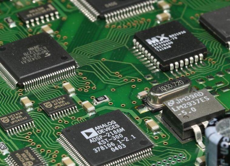
2. Device information
Draw the schematic from orcad, and then transfer out the allegro netlist. Double-click the device in orcad-capture and you can see that PCB footprints (part package) is assumed to be SO16 in the properties and HEF4051B in the source package (target device). Reflected in the netlist as SO16! HEF4051B: U01, the device file is generated from the principle from the capture-allegro netlist command. For example, SO16.txt will explain the device, pin and related information. SO16 refers to the package form, while HEF4051B is a real device.
Common package forms: DIP dual in-line package, QFP quad flat package, SOP small frame package, PLL leaded chip carrier, BGA ball grid array package, etc. Please refer to the relevant information for details. Design the pads and connection holes according to the data you get. Cadence PSD uses pad designer to design.
There are five categories of Pad types:
1, regular: solid graphics positive pad (black), can be round, square, ellipse.
2, thermal: relief flower-shaped graphics, instead of regular pads for better heat dissipation.
3, anti pad: negative pad (clear), usually cut off the circle in the square to prevent the pin from connecting to other metal layers.
4,shapes: user-defined graphics
5, flash: user-defined aperture
Via is called a via. If it passes through the entire board, it is a through via, if it only appears on one surface, it is a blind via, and if it is inside (not visible on both surfaces), it is a buried via.
The pads and vias set by pad designer will be used when building the symbol. Start allegro ->new->package symbol (wizard), enter the size, type and previously set pad of the corresponding device. (Note: The first pin must be identified), and then the symbols corresponding to the device will be generated. The names of these symbols must be consistent with the names of PCB footprints so that there is no error when assigning names. (Save as .dra file)
Start allegro->new->board to generate a motherboard file, draw the shape of the board with lines, and assign the keepin router/package as the place and wiring area, and save it as a .brd file. Then import-logic reads in the allegro netlist output from orcad. (If an illegal character is enclosed in single quotation marks, the brackets are comments).
After the input is successful, you can place the device (place manual), and use logic->logic-assign refdes to click and name the device. If it is correct, a flying line will appear. After the placement is successful, everyone can refer to the wiring strategy written by the masters for wiring and simulation.
3. Placement and connection of devices
Relatively speaking, there are many considerations for device placement, such as the direction of the board, the function of the device and related interference, the placement of special devices, the heat dissipation of the device, and the ease of wiring.