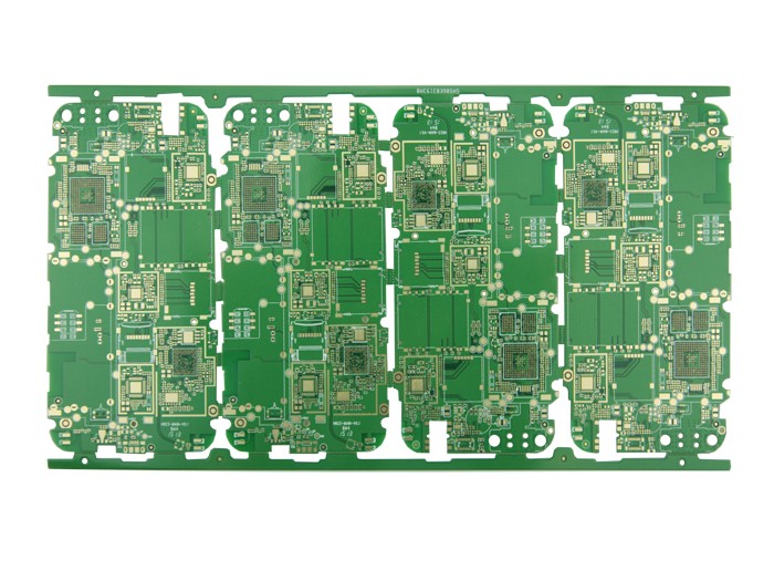
PCB board wiring can be said to be an art. An excellent circuit board design must consider all aspects, including the realization of circuit principles and functions, but also consider the electrical characteristics of EMI, EMC, ESD, signal integrity, etc., as well as the mechanical structure and the heat dissipation of high-power chips. Then consider the aesthetics of the circuit board. This is also important in our PCB copy board industry.
Before you start learning to explore PCB layout, you may see various rules for PCB layout in various reference books. Even though many rules may have the same connotation to a certain extent, they are different. There will be different emphases in actual layout practice, and there will even be conflicts between rules. For example: Rule one is that the signal transmission path is as short as possible, and rule two is that impedance matching is required in high-frequency wiring.
When considering the layout of the DDR MEMORY bus, it is impossible for the SOP packaged MEMERY chip to implement rule one for all TRACKs. The correct approach is to implement all the TRACKs in the relatively shortest under the condition of overall consideration of impedance matching. Therefore, the incompatibility between the rules in the actual wiring will cause the readers to consciously and effectively use these rules in the wiring process to produce all kinds of doubts, and even fall into this or that kind of general rules at a loss. This needs to be emphasized-the various wiring rules are only guidelines, and the actual wiring process should be combined with continuous compromises to achieve the greatest effect. I think that as long as you consciously pay attention to these rules in the actual wiring, it will more or less help the effect of the wiring.

1. From the perspective of the entire system, analyze the nature of each module signal and determine its position in the entire system, so as to determine the priority of the module in the layout and routing is of great significance to the entire system, which requires the actual wiring process In, the specific processing of each module is prioritized.
The general layout rules require to distinguish whether the module is an analog circuit or a digital circuit, whether it is a high-frequency circuit or a low-frequency circuit, whether it is a main interference source or a sensitive key signal, and so on. Therefore, it is necessary to carefully analyze the properties of each module signal before layout, including module attributes, functions, power supply, specific signal frequency, current flow, current intensity, etc., to determine the layout of the module on the PCB board. Usually, when the mechanical structure is determined, a complex system will have N different layout methods, which requires a compromise of some rules to find the optimal layout from the perspective of the system.
In the digital module, there will be a clock, such as the CLOCK of SDRAM, and the clock circuit is the main factor affecting EMC. Most of the noise of an integrated circuit is related to the clock frequency and its multiple harmonics. If the CLOCK signal is in the form of a sine wave, if it is not handled properly, it will “contribute” an interference source of this frequency or a multiple of this frequency to the system. If the CLOCK signal is in the form of a square wave, it will “contribute” a noise to the system. Disperse frequency interference source. At the same time, CLOCK is still a signal that is susceptible to interference. If CLOCK is interfered, the impact on the digital system can be imagined. Therefore, the clock circuit module is a key module, and various rules are given priority in the layout and routing process.
There are also various interrupt modules in many embedded hardware systems nowadays. Interrupt triggers include level trigger and edge trigger. Once encountered an interrupt that was set as a rising edge trigger was continuously triggered due to external interference, which eventually led to the phenomenon that the RTOS was blocked because it could not be processed.
Analyze two simple circuit layouts according to this principle. In a mobile phone hardware platform I came into contact with, the brightness circuit of the display screen is realized by using a PWM signal with different pulse widths, and an RC integrator circuit to establish different backlight voltages. Compared with CLOCK, the PWM signal has the same effect on the EMI of the entire system in a certain sense. But if you analyze some carefully, you should know that if the PWM signal of the IC establishes an analog level in the shortest possible path before being transmitted on the PCB board, that is to say, the resistance and capacitance are as close as possible to the PWM. Pin placement, so that the interference of PWM to the system can be reduced to a minimum. In the design of the mobile phone hardware platform, the RF part and the audio part are the core of the system, and the wiring of these two parts occupies the absolute core position, and puts it in a priority position when wiring. Therefore, in the actual layout and routing, the signal lines of these two modules are separately laid out in an intermediate layer, and the power layer and ground layer are used in the adjacent layer to shield it, and other modules are as far away as possible from these two modules to avoid introducing interference . In addition, try to consider such a detail: the audio signal with a very small MIC input needs to be amplified to a certain degree before being input to the AUDIO ADC. We know that the channel transmission signal-to-noise ratio in the abstract sense is a measure of the impact of noise on the system. It can be cross-referenced, a small noise crosstalks the channel before the audio signal is amplified and the audio signal enters the channel after the audio signal is amplified. If the path of this channel cannot pass through areas with strong interference sources, it is recommended that the audio signal be amplified before transmission.
For example, the bus of a complex system is usually connected to a type of device. For example, the I2C bus can be connected to 127 slave devices. In some set-top box hardware platforms, DEMODULATOR, TUNER, and E2PROM are usually connected. This also requires that different devices be distinguished in the frequency of sharing the bus, and the devices with a high frequency of use should be placed in a relatively important position. For example, the EMI interface on the above-mentioned QAMI5516 platform uses both SDRAM and FLASH devices. Based on the understanding of the system, SDRAM puts the running code of the real-time operating system, and FLASH is used as a storage medium. During the operation of the software system, SDRAM has more read and write operations than FLASH, so the wiring process should be done first. Consider the location of SDRAM.
2. The idea of modularization and structuring is not only reflected in the hardware principle design, but also reflected in the layout and routing effect. Today's hardware platforms are becoming more and more integrated, and the system is becoming more and more complex. Naturally, it is required whether it is a hardware schematic diagram. In the design of PCB layout, modular and structured design methods are still used. If you have been exposed to large-scale FPGAs or CPLDs, you know that the design of complex ICs inevitably requires a top-down modular design method. Therefore, as a hardware engineer, under the premise of understanding the overall architecture of the system, you should first consciously incorporate modular design ideas in the schematic and PCB wiring design. For example, the main IC of the hardware platform of the digital TV set-top box-QAMI5516 has the following modules: ST20: 32-bit RISC CPU clocked at 180MHZ
PTI: TRANSPORT STREAM processing unit DISPLAY: MPEG-2 decoding, display processing Unit DEMODULATOR: QAM demodulator MEMORY INTERFACE: Different MEMORY interfaces required by different application systems STBUS: Data communication bus of each module PERIPHERALS: UART, SMARTCARD, IIC, GPIO, PWM and other common peripherals AUDIO: Audio output interface VEDIO: The modular design process of the video output interface QAMI5516 does not necessarily require hardware engineers to understand all aspects of the system, but it inevitably requires that the interface parts of the different IC modules used in actual applications be regarded as a subsystem when designing the hardware platform. Processing: For example, the audio circuit and the video circuit should be carried out in a whole area during layout and wiring. Doing so not only continues the idea of IC modular design, but also facilitates physical separation of PCB boards when needed, reduces electrical coupling between different modules, and facilitates the debugging of the entire system. We know that it is the easiest to check in hardware debugging. The way to deal with errors in circuit principle design is to "treat your head and feet", that is, in the above-mentioned QAMI5516 platform, if there is a problem with the audio part of the circuit, the first thing to do is Check and verify the audio module.
The idea of modularization is also reflected in the wiring of the system bus. Usually, the bus is divided into three types: CONCROL BUS, DATA BUS, and ADDR BUS. For example, the SMI in the above QAMI5516 uses a 16M SDRAM with a working frequency of 100MHZ, which requires this group of buses to be unified into a whole to consider impedance matching during the wiring process. In the actual wiring process, it is impossible to lay out these lines sparsely.
The idea of modularization is also conducive to the layout of the PCB board.
The idea of modularization is also conducive to the expansion or modification of the hardware system's functions.
3. Pay attention to power supply integrity, and give priority to the processing of power and ground wires in layout and wiring. In any electronic system, the interference of interference sources on the system is nothing more than two ways: one is transmission through conductors, and the other is through space through electromagnetic radiation. Coupling. In low-frequency systems, it is mainly the first path. In high-frequency systems, a considerable part of the cause of interference is transmission through conductors. Among them, the more obvious is that the noise generated by IC interferes with the entire system through power and ground. Therefore, the integrity of the power supply or the quality of the power supply is of vital importance to the anti-interference ability of the entire system. Power integrity is actually a part of signal integrity, but considering the importance of power to all systems, it is listed separately here. It should be stated that it is not easy to do this in an actual system. There will always be noises of different frequencies in the system. In the circuit design and PCB layout and routing, it is only trying to reduce the noise of various frequencies, thereby improving the overall performance of the anti-noise of the system. At the same time, in a complex system, reducing the noise of the system is not to change the value of one or two capacitors, but to pay attention to the accumulation of power supply filtering effects. In the hardware design of mobile phones, there are dedicated PMUs to manage and supply power to each module, but the PMUs are all from VBAT. It is impossible to imagine that if the power supply of a sensitive audio op amp is not filtered and is directly taken from VBAT, or, like the circuit that supplies power to SDRAM, it is not filtered, and the switching noise of this part of the digital circuit is allowed to pollute the entire VBAT. What are the consequences?
If enough attention is paid to power integrity, this part is relatively easy to deal with after combining the modularization and careful analysis of each module mentioned above. The usual rules for IC power supply VCC are generally handled by bypass capacitors and decoupling capacitors, and try to keep these capacitors close to the power input of the IC when laying out the board. If you are in a demanding system, you can also use an LCCL circuit for different sensitive frequencies (connect an inductor or a magnetic bead in series, and an electrolytic capacitor, and a ceramic capacitor, and then a small inductor in series. The specific value needs to follow The corresponding frequency is determined) filtering. I used to make a complicated system. Because there is no bypass capacitor on the core power supply of the system's DEMODULATOR, the DEMODULATOR's bit error rate after demodulation is unbearable. For the processing of various GNDs in the system, it is generally required to analyze the return path of the current. The current has the property of always selecting the return path with the least impedance. This is a core principle, which can be understood by the fact that there is a pattern of "copper laying" in PCB wiring. "Paving copper" is often used on the network GND. All digital signals can be abstracted into a most basic gate-level circuit. GND is also a part of the signal return path. GND is to make the total impedance on the signal path smaller by "laying copper". "Nearby grounding" and "minimizing ground impedance" are also based on such considerations.
The above is the introduction of reasonable wiring in circuit board design. Ipcb is also provided to PCB manufacturers and PCB manufacturing technology.