If you are a computer hardware enthusiast, then you must be familiar with the term "PCB board". You can see it in most articles on computer motherboards and graphics cards: "For example, how many layers of PCB boards are used by a certain graphics card", "What color PCB board is used" and so on, so what exactly is a PCB board? What is the concept of the number of layers of the PCB board? Many friends are not clear about this, this article will answer these PCB board related questions for you.
What is a PCB board?
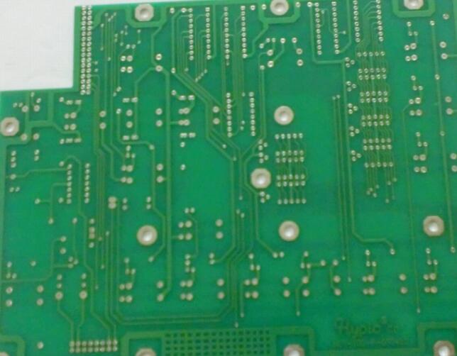
Speaking of PCB boards, it can be seen everywhere around us, from household appliances, various accessories in computers, to various digital products. As long as it is electronic products, almost all PCB boards are used. So what exactly is a PCB board? PCB board is the abbreviation of Printed Circuit Block, which is a printed circuit board for the placement of electronic components and a base board with circuits. The copper-plated base plate is printed on the anti-corrosion circuit by using the printing method, and the circuit is etched and washed out.
PCB board classification
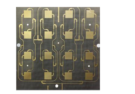
PCB boards can be divided into single-layer boards, double-layer boards and multi-layer boards. Various electronic components are integrated on the PCB. On the most basic single-layer PCB, the parts are concentrated on one side, and the wires are concentrated on the other side. In this case, we need to make holes in the board so that the pins can pass through the board to the other side, so the pins of the parts are soldered to the other side. Because of this, the front and back sides of such a PCB are called Component Side and Solder Side respectively.
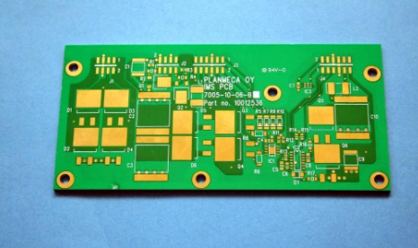
The double-layer board can be regarded as a combination of two single-layer boards relative to each other. There are electronic components and wiring on both sides of the board. Sometimes it is necessary to connect a single wire on one side to the other side of the board, which requires a via. A via is a small hole filled or coated with metal on the PCB, and it can be connected with wires on both sides. Many computer motherboards now use 4-layer or even 6-layer PCB boards, while graphics cards generally use 6-layer PCB boards. Many high-end graphics cards like the nVIDIA GeForce 4 Ti series use 8-layer PCB boards (the latest GeForce FX 5800Ultra even Using a 12-layer PCB), this is the so-called multi-layer PCB. On multi-layer PCB boards, there will also be problems connecting the lines between the various layers, which can also be achieved through vias. Because it is a multi-layer PCB, sometimes the vias do not need to penetrate the entire PCB. Such vias are called buried vias and blind vias, because they only penetrate a few layers. Blind holes are to connect several layers of internal PCB to the surface PCB, without having to penetrate the entire board. Buried vias only connect to the internal PCB, so they cannot be seen from the surface. In a multilayer PCB, the entire layer is directly connected to the ground wire and the power supply. So we classify each layer as signal layer, power layer or ground layer. If the parts on the PCB require different power supplies, this type of PCB usually has more than two layers of power and wire.
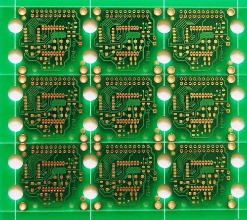
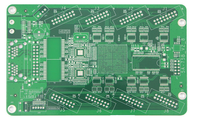
With the rapid development of electronic equipment, especially equipment around computers, products using 8-layer or even 12-layer PCB boards are already common products. Take graphics cards as an example: in order to adapt to a large number of electronic components and higher operating frequencies, It is very important to ensure signal synchronization and stability. Using more layers of PCB boards can effectively ensure signal stability and reduce interference. However, problems also follow. The more PCB layers, the more complicated the process and the higher the cost. Complicated technology will cause a certain rejection rate, which is why products with more than 8 layers of PCB boards are very rare.
PCB board production process
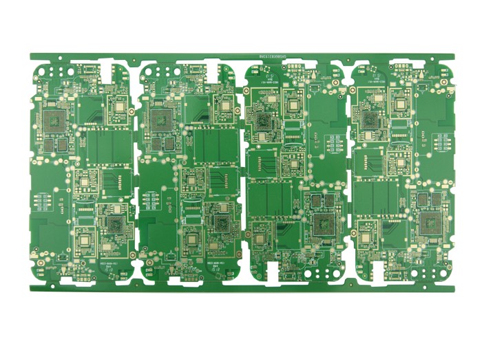
The production process of professional PCB boards is quite complicated. Take 4-layer PCB boards as an example (mainboard PCBs are mostly 4-layer). When manufacturing, the two middle layers are rolled, cut, etched, and oxidized. The four layers are the component surface, power layer, ground layer, and solder pressure layer. Put these 4 layers together and roll them into a motherboard PCB. Then punch and make through holes. After cleaning, print, copper, etch, test, solder mask, silk screen on the outer two layers of circuits. Finally, the entire PCB (including many motherboards) is stamped into a motherboard PCB, and then vacuum packaged after passing the test. If the copper is not well laid during the PCB manufacturing process, there will be a phenomenon of loose bonding, which is likely to imply short circuit or capacitive effect (easy to produce interference). The vias on the PCB must also be paid attention to. If the hole is not in the middle, but to one side, uneven matching will occur, or it will be easy to contact the power layer or ground layer in the middle, which will cause potential short circuits or poor grounding factors.
Copper wiring is a very important step in the production of PCB boards. The negative film transfer method is used to express the working film on the metal conductor. This technique is to spread a thin layer of copper foil on the entire surface and eliminate the excess part. Supplementary transfer is another method that less people use. It is a method of laying copper wires only where needed, but we won't talk about it here. Positive photoresist is made of sensitizer, which will dissolve under lighting. There are many ways to treat the photoresist on the copper surface, but the most common way is to heat it and roll it on the surface containing the photoresist. It can also be sprayed on the head in a liquid way, but the dry film type provides higher resolution and can also produce thinner wires. The hood is just a template for the PCB layer in manufacturing. Before the photoresist on the PCB board is exposed to UV light, the light shield covering it can prevent the photoresist in some areas from being exposed. These areas covered by photoresist will become wiring. After the photoresist is developed, the other bare copper parts to be etched. The etching process can immerse the board in the etching solvent or spray the solvent on the board. Generally used as an etching solvent, ferric chloride and the like are used. After the etching, the remaining photoresist is removed.
The above introduces the relevant knowledge of PCB. Through the above introduction, we know that PCB boards can be divided into single-layer, double-layer and multi-layer. Generally, individual electronic enthusiasts use single-layer PCB boards, which are cheap and easy to route., There is no need for any lead-through, and there are no special requirements for welding. Knowing these basic knowledge can give us a deeper understanding of the surrounding electronic equipment, and it would be even better if it can help you repair your electrical appliances.