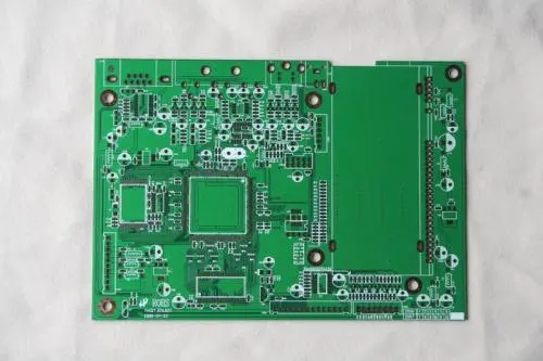
A 20-layer circuit board with a typical digital-analog hybrid circuit designed for 32-channel digital reception and conversion. The highest frequency is high-speed fiber optic signals up to 2.5GHz.

The printed circuit board layout separates the analog circuit from the digital circuit, and each channel is completely independent with a certain distance to ensure that the analog signals of each channel will not interfere with each other. Place the analog circuit as close to the edge of the circuit board as possible, and place the digital circuit as close as possible to the power connection end. This can reduce the di/dt effect caused by the digital switch.
In the division of power and ground, the analog signals of this PCB printed circuit board are all on the surface layer, and the holes should be as short and as few as possible. The second and nineteenth layers next to the analog signal are both complete and unified analog ground planes, so as to ensure that the analog signal has the best return path and impedance, and there will be no E M I problems across divisions. The high-speed signal layer is adjacent to the ground plane layer, and important signal lines are routed as strip lines, and the third layer is routed to the clock and reset sensitive signal lines, between the two ground planes. Both digital power and analog power have independent levels and are divided, but each power level is also adjacent to the ground plane.
High-speed A/D hybrid devices are connected to analog ground on the board, that is, the external ground pins of the device, and the power pins are connected to analog power, and decoupling capacitors are added next to the power pins to eliminate high-frequency interference. The wire on the magnetic bead inductance that is connected to the power supply or ground should be thicker. It is better to connect a few more signal wires to the power supply or ground plane. This can reduce the voltage drop and reduce the noise.
Sometimes, large via holes can be used to connect the plane to meet the requirements.
High-frequency signal lines are strictly controlled in line width and line spacing to meet the impedance requirements. They are all manually wired. Finally, dense holes are drilled in the blank area of a large area of copper foil in the analog circuit part to connect to the analog ground.
The 100M clock signal line on this printed circuit board has been simulated and analyzed by the design software, and the signal transmission is basically not disturbed, which meets the requirements of telecommunications. The printed circuit board produced has been debugged and showed that the digital signal has little interference to the analog signal, and the parameter index is good.
The above is the introduction of PCB design examples of hybrid circuits. Ipcb is also provided to PCB manufacturers and PCB manufacturing technology.