Plasma refers to light like purple light and neon light, and it also has a fourth phase called PCB copy boardmaterial. The plasma phase is due to the disordered movement of excited electrons and molecules in the atom, so it has a relatively high energy.

(1) Mechanism:
Applying energy (such as electric energy) to the gas molecules inside the vacuum chamber, the collision of accelerated electrons causes the outermost electrons of the molecules and atoms to be excited, and ions or highly reactive free radicals are generated.
The ions and free radicals generated in this way are accelerated by continuous collisions and electric field forces, causing them to collide with the surface of the material, and destroy molecular bonds within a few microns, induce a certain thickness reduction, generate a concave-convex surface, and form a gas component at the same time. The physical and chemical changes of functional groups and other surfaces can improve the copper plating adhesion and decontamination effects of PCB copying.
Oxygen gas, nitrogen gas and carbon tetrafluoride gas are commonly used for the above-mentioned plasma processing gas. The following uses a mixed gas composed of oxygen and carbon tetrafluoride gas to illustrate the mechanism of plasma treatment:
(2) Purpose:
1. Etching/de-hole wall resin contamination;
2. Improve surface wettability (Teflon surface activation treatment);
3, the treatment of the carbon in the blind hole by laser drilling;
4. Change the surface morphology and wettability of the inner layer to improve the bonding force between the layers;
5. Remove resist and solder mask residues.
(3) Example:
A. Activation treatment of pure polytetrafluoroethylene material
For the activation treatment of pure PTFE material, a single-step activation through hole process is adopted. Most of the gas used is a combination of hydrogen and nitrogen.
The board to be processed does not need to be heated, because the PTFE is processed to become active, and the wettability is increased. Once the vacuum chamber reaches the operating pressure, the working gas and RF power supply are activated.
It only takes about 20 minutes to process most pure PTFE PCB copy boards. However, due to the recovery performance of the PTFE material (return to a non-wetting surface state), the hole metallization treatment of electroless copper must be completed within 48 hours after the plasma treatment.
B. Activation treatment of filler-containing polytetrafluoroethylene material
For printed circuit boards made of filler-containing polytetrafluoroethylene materials (such as irregular glass microfibers, glass braided reinforced and ceramic-filled polytetrafluoroethylene composites), two-step processing is required.
The first step is to clean and micro-etch the filler. Typical operating gases for this step are carbon tetrafluoride gas, oxygen and nitrogen.
The second step is equivalent to the one-step PCB copying process used in the surface activation treatment of the aforementioned pure PTFE material.
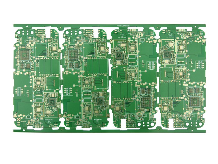
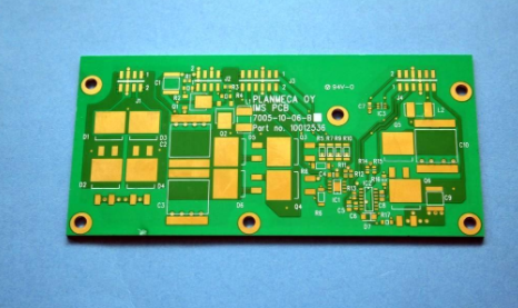
The above is the introduction of the plasma processing technology of PCB multilayer boards. Ipcb is also provided to PCB manufacturers and PCB manufacturing technology.