FiducialMarks and local fiducial marks are special PADs used by placement equipment for optical positioning.

Benchmark application
There are three situations for the application of reference symbols, 1) for the positioning of the entire PCB; 2) for the positioning of the PCB sub-boards of the imposition. 3) It is used for the positioning of fine-pitch devices. In this case, the QFP with a pitch of less than 0.5mm is recommended to set a positioning reference symbol at its diagonal position;
The type of reference point (Mark point type of reference point (Mark point).
Number of reference points
1) Two global fiducial marks are located at the opposite position of the diagonal of the PCB board, and as far away as possible; 2) At least two fiducial marks of the single board on each puzzle board are located on the diagonal of the PCB, and as far as possible keep away.
Datum point design of jigsaw
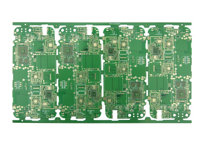
At least one pair of datums is designed on each single board; at least one pair of datums is designed on the whole board (the datums on the single board can be used instead of additional design); regardless of the datum point of the whole board or the datum point of the single board, the board The coordinates of the front and back sides of the PCB must be strictly the same relative to the corresponding datum at the lower left corner of the PCB puzzle. Otherwise it will cause patch errors! As shown below.
Benchmark shape and size
The best fiducial mark is a solid circle, size and deviation: A=1.0mm±5%? Around each identification mark, there must be an empty area without conductors, welding circuits, solder masks and other marks. The size of the empty area is more than 0.5mm larger than the external size of the identification mark. ? Flatness: The flatness of the surface of the fiducial mark should be within 15 microns [0.0006"].
In order to achieve the most accurate position of the reference point, the position of the reference point is best on the opposite corner of the substrate. And the farther the distance, the better. The reference point on the veneer should be at least 7.5mm away from the edge of the printed board and meet the minimum openness requirement of the reference point. Reference symbols are used in pairs. Arranged at the opposite corner of the positioning feature. ? Reference clearance (clearance) The reference clearance (clearance) around the reference point mark, there should be an open area without other circuit features or marks. The size of the open area should be equal to the radius of the mark. The reference point of the whole board must meet the requirement of openness, and the single base board is recommended to meet the requirement of openness of the reference point. ? The benchmark material is gold-plated, bare copper, nickel-plated or tin-plated, or solder coating (even hot air). Around the fiducial mark, there should be a clear area (Clearance) with no other circuit features or marks. The best performance can be achieved when there is a high contrast between the fiducial mark and the substrate material of the printed board.
localFiducial
When the number of pins of the mounted device is large, and the pin spacing is ≤0.5mm, it is recommended to design a set of graphics for the optical positioning of a single device, that is, a local fiducial mark, which is recommended.
The design of SMT printed board vias and pads The design of SMT printed board vias and pads
Pad vias 1) In principle, the pad should be avoided as far as possible to design vias. 2) If a via is used on the pad, the smaller the diameter of the via, the better, and at the same time, the via is completely filled.
Via layout
The distance between the via hole and the pad without solder mask treatment is ≥ 0.3mm. If the via hole has been solder mask treated, there is no requirement for the distance between the via hole and the pad. Note: Due to capillary action, the vias may suck the molten solder away from the components, resulting in insufficient solder joints or false soldering. Unfilled vias will cause solder paste application and poor soldering.
Four PCB pad design process requirements pad design process requirements
An extremely critical part of circuit design. Pad design is an extremely critical part of PCB circuit design, because it determines the welding position of the component on the printed board, and determines the welding position of the component on the printed board, and It plays an important role in the reliability of the solder joints, such as welding defects that may occur during the welding process, cleanability, performance, welding defects that may occur during the welding process, cleanability, and measurable maintenance. Trial and visual inspection, maintenance, etc. play an important role.
Pad pitch
Taking into account the component manufacturing error, placement error, inspection and rework, considering the component manufacturing error, placement error, and inspection and rework, the spacing between the pads of adjacent components should be designed according to the following principles: adjacent components The spacing between the device pads should be designed according to the following principles:
IC component side Chip component frame Chip component ≥0.3㎜IC component frame shielding cover≥0.3㎜≥0.5㎜≥0.3㎜≥0.5㎜≥0.5㎜≥0.5㎜Printed board edge ≥0.3㎜Shielding cover ≥0.5㎜≥0.5㎜≥ 0.5㎜≥0.5㎜Special-shaped component ≥0.5㎜
The distance between ≥The distance between the discharge tube and the adjacent element PAD ≥0.4 mm The distance between the discharge tube and the discharge tube ≥0.1mm The distance between the discharge tube and the discharge tube ≥0.1mm
Description: Description: Components: Chip components: 0201, 0402, 0603 and other components; Components: IC components: BGA, QFP, QFN, aQFN and other components; Special-shaped components: Special-shaped components: earphone sockets, side keys, battery connectors, T Cards and other components; shielding cover: shielding cover: refers to the inner and outer edges of the shielding cover pad. As long as the mounting density allows, the above distance should be as large as possible. As long as the mounting density allows, the above distance should be as large as possible.
CHIP component pad design CHIP component pad design
Chip component pad design should master the following key elements: Chip component pad design should master the following key elements: Component pad design should master the following key elements a) Symmetry-the pads at both ends must be symmetrical to ensure the surface tension of molten solder balance. b) Pad spacing-ensure the proper overlap size of the component end or pin and the pad. c) The remaining size of the pad-the remaining size after the overlap must ensure that the solder joint can form a meniscus. d) The width of the land-should be basically the same as the width of the component tip or pin.
4. Edge flat package device (QFP) pad design edge flat package device (QFP)
Pitch pad width (mm) pad length (mm)
0.80.51.8
0.650.41.8
0.50.31.6
0.40.251.6
0.30.171.6
The land design of the quad flat no-lead plastic package (PQFN) and the five-quad flat no-lead plastic package (PQFN)
Two types of PQFN conductive pads Two types of PQFN conductive pads
1) One type only exposes the bottom side of the package, the bottom side, and the other parts are packaged in the component. Is encapsulated in the component.
2) Another type of pad has a part that is exposed on the side of the package.
3) Design of large area thermal pad ≈ device large area exposed pad size, also need to consider avoiding and surrounding large area thermal pad design ≈ device large area exposed pad size, edge pad bridging and other factors. Edge pad bridging and other factors. 4) The size of the conductive pad is similar to the corresponding pad around the device, but the size of the conductive pad is slightly longer than the corresponding pad around the device, and it is longer (0.3~0.5mm). Longer (0.3~0.5mm).
IC and BGA pad design IC and BGA pad design
BGA pad design: BGA pad design: The pad design is based on the relevant nominal value provided by the supplier, and the pad design is performed on the size; 1) According to the relevant nominal value provided by the supplier, the solder is performed on the size Disk design: The pad surface treatment uses OSP to ensure the flatness of the mounting surface, OSP, 2) The pad surface treatment uses OSP, which can ensure the flatness of the mounting surface and allow the components to be properly self-centered. Gold plating should be avoided, because during reflow soldering, there will be a reaction between the solder and gold, which is self-centering. Gold plating should be avoided, because during reflow soldering, there will be a reaction between the solder and gold, which weakens the connection of the solder joints; weakens the connection of the solder joints; try not to place the vias on the pads, such as the positive and negative sides. Holes and vias need to be plugged; 3) Try not to place vias on the pads. For example, if there are vias on the front and back sides, the vias need to be plugged; if there is space between the pads, a solder mask can be used. Make a solder mask. 4) If there is space between the pads, a solder mask can be used, and a solder mask must be made. Other requirements of BGA: Other requirements of BGA: the drawing method of the outline positioning line should be standard; 5) The drawing method of the outline positioning line should be standard; when there are multiple BGABGAs when the chip position is arranged, 6) when there are multiple BGAs, When arranging the chip position, consider processability; consider reworkability, usually leave more than 1mm around the BGA; recommended) leave more than 1mm around the BGA 7) consider reworkability, usually leave more than 1mm around the BGA; (recommended) for lead spacing ≤0.5mm QFP and ball pitch 0.5mm BGA packaged devices and ball pitch ≤ packaged devices. 8) For QFP with lead pitch ≤0.5mm and ball pitch ≤0.5mm BGA packaged devices, in order to improve the sticker
Chip accuracy requires setting reference points on two diagonal corners of the IC. Chip accuracy requires setting reference points on two diagonal corners of the IC. Set the reference point on the two diagonals of the IC
0.5mmPitchBGA Pad
1) The pad center of each solder ball on the PCB and the pad center of each solder ball on the PCB coincide with the center of the corresponding solder ball at the bottom of the BGA; the center of the corresponding solder ball at the bottom coincides with the center of each solder ball on the The center of the pad matches the center of the corresponding solder ball at the bottom. 2) The PCB pad pattern is a solid circle, and the via hole cannot be processed on the pad; the pad pattern is a solid circle, and the pad pattern is a solid circle. Processed on the pad; a maximum diameter of the pad is equal to the maximum diameter of the pad equal to the diameter of the land of the BGA bottom solder ball; (recommended) the diameter of the bottom solder ball; recommended) the minimum diameter of the bottom solder ball is equal to The minimum diameter is equal to the diameter of the bottom pad of the BGA minus the placement accuracy. (Recommended) The bottom pad diameter minus the placement accuracy. Recommended) The bottom pad diameter minus the placement accuracy. For example: the bottom pad diameter is 0.3mm, the placement accuracy is ±0.05mm, PCB soldering. For example: the BGA bottom pad diameter is the bottom pad diameter, and the placement accuracy is ±, The minimum diameter of the pad is 0.30mm-0.05mm. (. (The pad diameter of the solder ball at the bottom of the BGA device is based on the minimum diameter of the disk. (The pad diameter of the solder ball at the bottom of the device is based on the information provided by the supplier) The information provided by the supplier) 3) The solder mask size is larger than the pad size~ 0.15mm. The solder mask size is 0.1~ larger than the land size.
0.45mmPitch&0.27mm ball diameter of aQFN (MT6253) pad ball diameter
The recommended pad size is 0.27mm, the solder mask window size is recommended, and the solder mask window size is recommended to be 0.37-0.4mm. .
The close-pitch IC of the close-pitch PAD and the close-pitch IC increase the copper skin and increase the attractive force of the side pins, which facilitates self-centering of reflow soldering and prevents continuous soldering.
J-pin small-outline integrated circuit (SOJ) and plastic-packaged leaded chip carrier (PLCC) solder-shaped pin small-outline integrated circuit (shaped pin small-outline integrated circuit) and plastic packaged leaded chip carrier () plate design The pins of SOJ and PLCC are both J-shaped, and the typical pin center distance is 1.27mm; a) Single pin pad design (0.50~0.80mm)*(1.85~2.15mm); b) The center of the pin should be soldered Between the inner 1/3 of the disk pattern and the center of the pad; c) The distance between the SOJ relative to the two rows of pads (the inner outline of the pad pattern) A value is generally 5, 6.2, 7.4, 8.8 (mm); d) PLCCPLCC Relative distance between two rows of pad outlines: J=C+K (unit: mm) where: J-pad pattern outline distance;
KeyPad designKeyPad design
KeyPad requirements in principle: KeyPad requirements in principle: in principle, it is required to design as a complete concentric circle as much as possible, and no mechanical holes; 1) Design as a complete concentric circle as far as possible, and no mechanical holes; each concentric The diameter of the circle shall not be less than φ5mmφ5mm; 2) The diameter of each concentric circle shall not be less than φ5mm; the distance between the closest points of adjacent KeyPad is ≥0.2mm; the distance between the closest points of KeyPad 3) the distance between the closest points of adjacent KeyPad ≥0.2mm; There should be no surface wiring in the area covered by the pot, and laser vias are used for wiring. 4) There should be no surface wiring in the area covered by the DOME pot, and laser vias are used for wiring. There must be at least two exposed copper near the KeyPad for DOME grounding. At least two exposed copper near the KeyPad must be used for DOME grounding. 5) There must be at least two exposed copper near the PCBKeyPad for DOME grounding. If the PCB size is small, it is impossible to make a complete and complete KeyPad with concentric circles. The PCB size is small due to the small size of the PCB. If it is impossible to make a complete and complete KeyPad with concentric circles due to the small PCB size, you need to consider the DOME pot. The problem of cooperation between the pot and the KeyPad: reduce the size of the pot so that after pressing, the coordination problem of the DOME pot and the KeyPad needs to be considered. Edges or heterosexual edges cannot exceed the straight edges and irregular edges of the KeyPad. The straight or heterosexual side of the KeyPad straight edge and profiled edge cannot exceed the KeyPad straight edge and profiled edge. It can avoid that the side of the pot repeatedly rubs the solder mask on the PCB, causing the copper under the solder mask and the pot to short circuit, causing the KeyPad to fail. The solder mask on the upper side, the KeyPad fails the solder mask on the PCB, causing the copper and the pot under the solder mask to short circuit, causing the KeyPad to fail.
Outline positioning line (silk printing frame) When drawing the device graphics of the outline positioning line (silk printing frame), it is necessary to draw the external frame graphics of the component. 1) When drawing the BGA device graphics, the external frame graphics of the component must be drawn. The purpose is to center during inspection. . Centering. For components related to structural coordination such as battery sockets, cards, etc. 2) For components related to structural coordination such as battery sockets, SIM cards, etc., the outline positioning frame of the components must be added when making the PCB board, which is the silk screen block diagram., The outline positioning frame of the components must be added when boarding, which is the silk screen block diagram, and gold wire can also be used as the outline positioning frame. Bit frame. For the patch structure, components with positioning holes are preferred. 3) Components with positioning holes are preferred for SMD structural parts.
The above is the introduction of PCB design positioning reference symbols and dimensions. Ipcb is also provided to PCB manufacturers and PCB manufacturing technology.