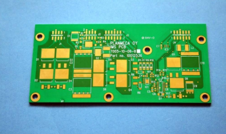
PCB wiring is a key element of ESD protection. A reasonable PCB design can reduce unnecessary costs caused by fault inspection and rework. In PCB design, because the transient voltage suppressor (TVS) diode is used to suppress the direct charge injection caused by ESD discharge, it is more important in PCB design to overcome the electromagnetic interference (EMI) electromagnetic field effect generated by the discharge current. This article will provide PCB design guidelines that can optimize ESD protection.

Circuit loop
The current enters the circuit loops through induction. These loops are closed and have varying magnetic fluxes. The magnitude of the current is proportional to the area of the ring. A larger loop contains more magnetic flux and therefore induces a stronger current in the circuit. Therefore, the loop area must be reduced.
The most common loop is shown in Figure 1, formed by power and ground. Where possible, a multi-layer PCB design with power and ground planes can be used. The multi-layer circuit board not only minimizes the loop area between the power supply and the ground, but also reduces the high-frequency EMI electromagnetic field generated by the ESD pulse.
If a multilayer circuit board cannot be used, then the wires used for power and ground must be connected into a grid as shown in Figure 2. Grid connection can play the role of power and ground layer. Use vias to connect the printed lines of each layer. The interval between vias in each direction should be within 6 cm. In addition, when wiring, placing the power and ground traces as close as possible can also reduce the loop area.
Another way to reduce the loop area and induced current is to reduce the parallel paths between interconnected devices.
When a signal connection line longer than 30 cm must be used, a protective line can be used, as shown in Figure 5. A better way is to place a ground plane near the signal line. The signal wire should be within 13 mm of the protection wire or ground wire layer.
As shown in Figure 6, the long signal line (>30 cm) or power line of each sensitive element and its ground line are cross-arranged. The crossing wires must be arranged at regular intervals from top to bottom or from left to right.
Circuit wiring length
Long signal lines can also become antennas for receiving ESD pulse energy. Try to use shorter signal lines to reduce the efficiency of signal lines as antennas for receiving ESD electromagnetic fields.
Try to place the interconnected devices in adjacent positions to reduce the length of the interconnected traces.
Ground charge injection
The direct discharge of ESD to the ground layer may damage sensitive circuits. While using TVS diodes, one or more high-frequency bypass capacitors are also used. These capacitors are placed between the power supply and ground of the vulnerable components. The bypass capacitor reduces charge injection and maintains the voltage difference between the power supply and the ground terminal.
The TVS shunts the induced current and maintains the potential difference of the TVS clamping voltage. TVS and capacitors should be placed as close as possible to the protected IC (see Figure 7), and the length of the TVS to ground path and capacitor pin length should be the shortest to reduce parasitic inductance effects.
The connector must be mounted to the copper platinum layer on the PCB board. Ideally, the copper-platinum layer must be isolated from the ground plane of the PCB and connected to the pad through a short wire.
Other guidelines for PCB design
Avoid arranging important signal lines on the edge of the PCB board, such as clock and reset signals;
Set the unused part on the PCB board as a ground plane;
The distance between the chassis ground wire and the signal wire is at least 4 mm;
Keep the aspect ratio of the chassis ground wire less than 5:1 to reduce the inductance effect;
Use TVS diodes to protect all external connections;
Parasitic inductance in the protection circuit The parasitic inductance in the TVS diode path can cause severe voltage overshoot in the event of an ESD event. Although TVS diodes are used, due to the induced voltage VL=L*di/dt at both ends of the inductive load, the excessive overshoot voltage may still exceed the damage voltage threshold of the protected IC.
The total voltage that the protection circuit bears is the sum of the clamping voltage of the TVS diode and the voltage generated by the parasitic inductance, VT=VC+VL. An ESD transient induced current can reach its peak value in less than 1ns (according to the IEC 61000-4-2 standard). Assuming that the lead inductance is 20nH per inch and the line length is a quarter of an inch, the overshoot voltage will be 50V /10A pulse. The empirical design criterion is to design the shunt path as short as possible to reduce the effect of parasitic inductance.
All inductive paths must consider the use of ground loops, the path between the TVS and the protected signal line, and the path from the connector to the TVS device. The signal wire to be protected should be directly connected to the ground plane. If there is no ground plane, the connection of the ground loop should be as short as possible. The distance between the ground of the TVS diode and the ground point of the protected circuit should be as short as possible to reduce the parasitic inductance of the ground plane.
Finally, the TVS device should be as close as possible to the connector to reduce transient coupling into nearby lines. Although there is no direct path to the connector, this secondary radiation effect will also cause the work of other parts of the circuit board to be disordered.