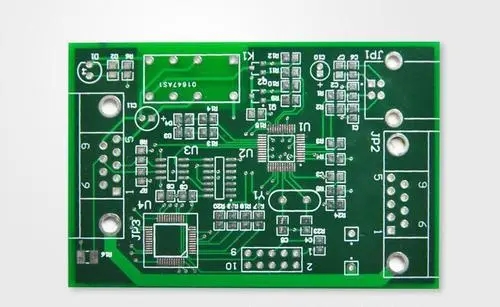
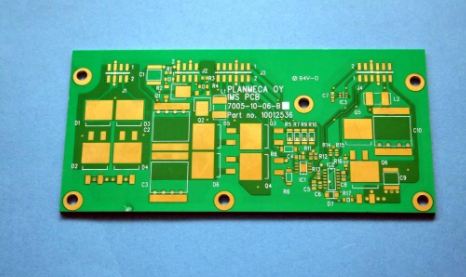
Component packaging summary
The component package not only plays the role of mounting, fixing, sealing, protecting the chip and enhancing the electrothermal performance, but also connects the pins of the package shell with wires through the contacts on the chip, and these pins pass through the printed circuit board. The wires are connected with other devices to realize the connection between the internal chip and the external circuit. Because the chip must be isolated from the outside world to prevent impurities in the air from corroding the chip circuit and causing electrical performance degradation. On the other hand, the packaged chip is also easier to install and transport. Since the quality of packaging technology also directly affects the performance of the chip itself and the design and manufacture of the PCB (printed circuit board) connected to it, it is very important.

An important indicator to measure whether a chip packaging technology is advanced or not is the ratio of chip area to package area. The closer this ratio is to 1, the better. The main considerations when packaging:
1. The ratio of the chip area to the package area is to improve the packaging efficiency, as close as possible to 1:1;
2, the pins should be as short as possible to reduce the delay, and the distance between the pins should be as far as possible to ensure that they do not interfere with each other and improve performance;
3. Based on heat dissipation requirements, the thinner the package, the better.
Packages are mainly divided into DIP dual in-line and SMD chip packages. In terms of structure, the package has experienced the earliest transistor TO (such as TO-89, TO92) package development to dual-in-line package, and then PHILIP company developed a small SOP package, and then gradually derived SOJ (J-type Lead small outline package), TSOP (thin small outline package), VSOP (very small outline package), SSOP (reduced SOP), TSSOP (thin reduced SOP) and SOT (small outline transistor), SOIC (small outline package) Integrated circuits) and so on. In terms of materials and media, including metals, ceramics, plastics, and plastics, many circuits that require high-strength working conditions, such as military and aerospace levels, still have a large number of metal packages.
The package has roughly gone through the following development process:
Structure: TO->DIP->PLCC->QFP->BGA ->CSP;
Materials: metal, ceramics -> ceramics, plastics -> plastics;
Pin shape: long lead in-line -> short lead or no lead mount -> ball bump;
Assembly method: Through-hole insert->surface assembly->direct installation
Specific package form
1, SOP/SOIC package
SOP is the abbreviation of English Small Outline Package, that is, small outline package. SOP packaging technology was successfully developed by Philips from 1968 to 1969, and later gradually derived SOJ (J-pin small outline package), TSOP (thin small outline package), VSOP (very small outline package), SSOP (reduced type) SOP), TSSOP (thin reduced SOP), SOT (small outline transistor), SOIC (small outline integrated circuit), etc.
2, DIP package
DIP is English Double In-line
The abbreviation of Package, that is, dual in-line package. One of the plug-in packages, the pins are drawn from both sides of the package, and the package materials are plastic and ceramic. DIP is the most popular plug-in package, and its applications include standard logic ICs, memory LSIs, and microcomputer circuits.
3, PLCC package
PLCC is the abbreviation of Plastic Leaded Chip Carrier in English, that is, plastic J-lead chip package. The PLCC package has a square shape and a 32-pin package with pins on all sides. The size is much smaller than that of the DIP package. The PLCC package is suitable for installing and wiring on the PCB with SMT surface mounting technology, and has the advantages of small size and high reliability.
4, TQFP package
TQFP is the abbreviation of thin quad flat package in English, that is, thin plastic package quad flat package. The quad flat package (TQFP) process can effectively use space, thereby reducing the space requirements of the printed circuit board. Due to the reduced height and volume, this packaging process is very suitable for applications with high space requirements, such as PCMCIA cards and network devices. Almost all CPLD/FPGA of ALTERA has TQFP package.
5, PQFP package
PQFP is the abbreviation of Plastic Quad Flat Package in English, that is, plastic quad flat package. The distance between the pins of the PQFP package is very small, and the pins are very thin. Generally, large-scale or ultra-large-scale integrated circuits use this type of package, and the number of pins is generally more than 100.
6, TSOP package
TSOP is the abbreviation of English Thin Small Outline Package, that is, thin small outline package. A typical feature of TSOP memory packaging technology is to make pins around the packaged chip. TSOP is suitable for mounting wiring on PCB (printed circuit board) using SMT technology (surface mount technology). In the TSOP package size, the parasitic parameters (when the current changes greatly, the output voltage will be disturbed) are reduced, which is suitable for high-frequency applications, and the operation is more convenient and the reliability is relatively high.
7, BGA package
BGA is the abbreviation of English Ball Grid Array Package, that is, ball grid array package. With the advancement of technology in the 1990s, chip integration continued to increase, the number of I/O pins increased sharply, power consumption also increased, and the requirements for integrated circuit packaging became more stringent. In order to meet the needs of development, BGA packaging began to be used in production.
The memory packaged with BGA technology can increase the memory capacity by two to three times without changing the volume of the memory. Compared with TSOP, BGA has a smaller volume, better heat dissipation performance and electrical performance. BGA packaging technology has greatly improved the storage capacity per square inch. With the same capacity, memory products using BGA packaging technology are only one-third of the volume of TSOP packaging; in addition, compared with traditional TSOP packaging, BGA packaging There is a faster and more effective way to dissipate heat.
The I/O terminals of the BGA package are distributed under the package in the form of circular or columnar solder joints. The advantage of BGA technology is that although the number of I/O pins has increased, the pin spacing has not decreased but increased. Improve the assembly yield; although its power consumption increases, but BGA can be welded with a controlled collapse chip method, which can improve its electrothermal performance; thickness and weight are reduced compared with the previous packaging technology; parasitic parameters are reduced, The signal transmission delay is small, and the frequency of use is greatly improved; the assembly can be coplanar welding, and the reliability is high.
The above is the introduction of component packaging inPCB design. Ipcb is also provided to PCB manufacturers and PCB manufacturing technology.