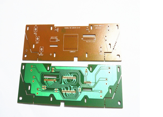
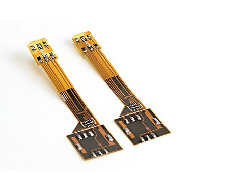
Nowadays, the development of mobile phones is becoming more and more intelligent, light and thin, which means that the internal components of mobile phones will also be further reduced or integrated. Under this development trend, the soft board (FPC) and class load in the PCB There are opportunities for further promotion and application of SLP. Related manufacturers are expected to follow the traditional peak season in the second half of the year. Consumer electronic products will be sourcing and their operations will continue to rise.
Thanks to the upcoming announcement of Apple’s new machine and the successive mass production and shipment of new products, the related supply chain revenue has also seen significant growth. Not only did the second quarter have a good performance, the July revenue also has an atmosphere of entering the peak season. For example, the cumulative revenue of Zhending and Taijun in the first 7 months has reached the second highest during the same period, while Yaohua and Huatong have set new highs during the same period.
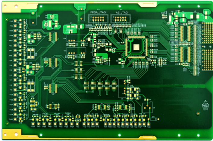
With the trend of thinner circuits, the HDI circuit process must be changed from the subtractive method to the modified semi-additive method (mSAP), or even an advanced semi-additive method using thinner CCL copper thickness (3μm) and 1μm copper thickness.

Additive method (amSAP) in order to achieve the purpose of finer lines. Although only Apple and Samsung have adopted similar carrier boards in smart phones so far, many circuit board manufacturers still predict that it is an inevitable trend that the line width/line spacing of mobile phone motherboards will be 15μm ∼20μm, and other mobile devices such as smart watches also have The application potential, so I am willing to take risks to invest in new equipment to build mSAP production lines.
The technological development and market application of HDI are also being driven forward at the same time. For example, in the demand for technological development, the thinner the circuit, the more important the mSAP process, the smaller the μVia aperture (50μm), the use of Pico Second or Femto Second laser drilling machine to reduce the thermal effect area, the aperture ratio must also reach About 0.8~1, and the Fan Out Wafer Lever Package (Fan Out Wafer Lever Package) circuit board with the chip must have very low warpage requirements, etc., all of which rely on the PCB manufacturer to invest resources from the material side and the equipment side.
From the perspective of the PCB market, in addition to smart phones as the largest application, other portable devices such as smart watches are also potential application markets. In the current industry competition, land-based circuit board manufacturers have gradually entered the HDI market, despite the production capacity and technology There is still a gap with Taiwan, Japan, Europe and the United States and other countries, but it also invisibly forces leading PCB manufacturers to move to higher-level SLP product layouts (on the other hand, of course, there is also substantial demand from Apple) to avoid falling prices. Competitive product belt, so although there are not many applications of SLP at present, when more and more SLP technologies and production capacity are in place, it will naturally drive more SLP applications. In other words, SLP has been driven by demand from the beginning. In the future, it may change to a situation where supply stimulates demand.