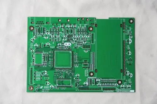
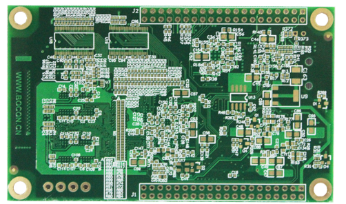
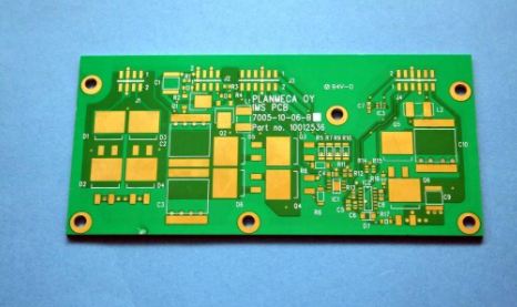
Some time ago, we invited everyone from Benqiang PCB Design Division to explain the knowledge of PCB design and board manufacturing. Starting from today, we will successively invite some well-known quality control experts in the quality control department of Benqiang Circuits to explain the quality control issues of PCB circuit boards. Help all the friends to get a good eye and uncover all kinds of "magic sprites" in the PCB industry.

Due to various uncontrollable factors, various problems will appear in the production process of PCB circuit boards, and some will seriously affect the quality of the circuit boards. Generally speaking, there are mainly the following "demons" in the PCB industry.
• Surface defects: such as burrs, nicks, scratches, grooves, broken fibers, exposed fabric, and voids.
• Surface defects: such as foreign inclusions, white spots/microcracks, delamination, pink circles, and voids in the laminate.
• Conductive pattern defects: such as lack of adhesion, reduction of conductor width and thickness due to nicks, pinholes, scratches, surface plating or coating defects, etc.
• Hole characteristics: such as hole diameter, misalignment, foreign inclusions, plating or coating defects and scratches.
• Marking anomalies: including location, size, readability and accuracy.
• Defects in the surface coating of the solder mask: such as misalignment, blistering, air bubbles, delamination, adhesion, physical damage and thickness.
• Size characteristics: including the size and thickness of the printed circuit board, aperture and pattern accuracy, conductor width and spacing, coincidence degree and ring width.
Today we will first understand the edge defects of the PCB circuit board.
As the name suggests, circuit board edge defects are defects such as burrs, nicks, or halos along the edge of the printed board. No one is perfect. Due to some uncontrollable factors, it is acceptable as long as they do not exceed the following requirements.
1. Burr
Burr is defined as small irregular block or mass protrusions protruding from the surface. It is the result of mechanical processing, such as drilling or milling.
1.1 Non-substantial thorns
Ideal edge of PCB circuit board
Ideal target-level 3, 2, 1
• Edge conditions-smooth, without burrs.
Acceptable conditions-level 3, 2, 1
• Edge condition-rough but not worn.
• Edge conditions-there are loose burrs, but does not affect the installation and function.
Not eligible-level 3, 2, 1
• The defect does not meet or exceed the above requirements.
1.2 The thorns
Target condition/acceptable condition-level 3,2,1
• The edges should be cut neatly without metal burrs.
Not eligible-level 3, 2, 1
• The defect does not meet or exceed the above requirements.
2. Gap
Target conditions-Level 3, 2, 1
• Edge conditions-smooth, no gaps.
Acceptable conditions-level 3, 2, 1
• The edges are rough but not worn.
• When the edge distance design complies with IPC-2222, the notch depth is not large
50% or 2.5 mm between the edge of the printed board and the nearest conductor
[0.0984 in], whichever is smaller.
• When the edge distance design does not comply with IPC-2222, the gap between the edge of the printed board and the nearest conductor distance need to be negotiated between the supplier and the buyer.
3. Halo
• When the edge distance is designed to comply with IPC-2222, the range of the halo is such that the unaffected distance between the edge of the board and the nearest conductive pattern is not less than the smaller of the two.
• When the edge distance design does not comply with IPC-2222, the distance between the halo and the nearest conductive pattern needs to be negotiated between the supplier and the buyer.
Not eligible-level 3, 2, 1
• The defect does not meet or exceed the above requirements