iPhone7 is about to come out, everyone is paying attention to Phone7’s gorgeous curved screen, cool 3D touch technology action, anticipated waterproof function and wireless charging technology, and its black technology makes people look forward to it, but these discussions are all It is more superficial, let us analyze its essence through these cool appearance functions, for example, its very key "skeleton"-the circuit board, the scientific name PCB.
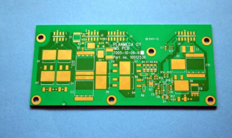
PCB (Printed Circuit Board), the Chinese name is printed circuit board, also known as printed circuit board. It is an important electronic component, a support for electronic components, and a carrier for electrical connection of electronic components. Because it is made by electronic printing, it is called a "printed" circuit board. Before the advent of PCB, the connection between electronic components was completed by direct connection of wires; but now, the wire connection method is only used in laboratory tests, and PCB has occupied the jue's control position in the electronics industry.
Talk about history, the past and present of PCB
From the beginning of the 20th century to the end of the 1940s, it was the embryonic stage of the development of the PCB substrate material industry. Its development characteristics are mainly manifested in: a large number of resins, reinforcing materials and insulating substrates used for substrate materials during this period have emerged, and preliminary explorations have been made in technology. These have created the necessary conditions for the advent and development of copper clad laminates, the most typical substrate material for printed circuit boards. On the other hand,

PCB manufacturing technology with metal foil etching (subtractive method) manufacturing circuits as the mainstream has been established and developed at the beginning. It plays a decisive role in the determination of the structural composition and characteristic conditions of the copper clad laminate.
The development history of PCB can be traced back to the early 20th century. In 1936, the Austrian Paul Eisler (Paul Eisler) applied PCB in the radio, putting PCB into practical use for the first time; in 1943, the United States widely used the technology in military radios; in 1948, the United States officially recognized that the invention can be used business use. As a result, PCB began to be widely used since the mid-1950s, and then entered a period of rapid development.
As PCBs become more and more complex, when designers use development tools to design PCBs, it is easy to confuse the definition and purpose of each layer. When our hardware developers draw the PCB by themselves, it is easy to cause unnecessary misunderstandings in production because they are not familiar with the purpose of each layer of the PCB. In order to avoid this situation, take AltiumDesignerSummer09 as an example to classify and introduce each PCB layer.
Differences between PCB layers
Signal Layer (SignalLayers)
AltiumDesignerzui can provide up to 32 signal layers, including the top layer (TopLayer), bottom layer (BottomLayer) and middle layer (Mid-Layer). The layers can be interconnected through vias (Via), blind vias (BlindVia) and buried vias (BuriedVia).
1. The top signal layer (TopLayer)
Also called the component layer, it is mainly used to place components. For double-layer boards and multilayer boards, it can be used to arrange wires or copper.
2. BottomLayer
Also called soldering layer, it is mainly used for wiring and soldering. For double-layer boards and multilayer boards, it can be used to place components.
3.Mid-Layers
There can be up to 30 layers, which are used to arrange signal lines in a multilayer board. Power lines and ground lines are not included here.
Internal power plane (InternalPlanes)
Usually referred to as the inner electric layer for short, it only appears in multi-layer boards. The number of PCB board layers generally refers to the sum of the signal layer and the inner electric layer. Same as the signal layer, the inner electric layer and the inner electric layer, and the inner electric layer and the signal layer can be connected to each other through through holes, blind holes and buried holes.
SilkscreenLayers
A PCB board can have up to 2 silk screen layers, namely the top silk screen layer (TopOverlay) and the bottom silk screen layer (BottomOverlay), generally white, mainly used to place printed information, such as component outlines and annotations, various notes Characters, etc., to facilitate the soldering of PCB components and circuit inspection.
1. Top screen printing layer (TopOverlay)
It is used to mark the projection outline of the components, the label, the nominal value or the model of the component, and various annotation characters.
2. Bottom Overlay
Same as the top silk screen layer, if all the marks on the top silk screen layer are included, the bottom silk screen layer can be closed.
Mechanical Layers (MechanicalLayers)
The mechanical layer is generally used to place indicative information about board manufacturing and assembly methods, such as the outline dimensions of the PCB, size markings, data materials, via information, assembly instructions and other information. This information varies according to the requirements of the design company or PCB manufacturer. The following examples illustrate our common methods.
Mechanical1: Generally used to draw the frame of the PCB as its mechanical shape, so it is also called the shape layer;
Mechanical2: We used to place the PCB processing process requirement form, including information such as size, plate, and layer;
Mechanical13&Mechanical15: The body size information of most components in the ETM library, including the three-dimensional model of the component; for the sake of simplicity of the page, this layer is not displayed by default;
Mechanical16: The footprint information of most components in the ETM library can be used to estimate the PCB size in the early stages of the project; for the simplicity of the page, this layer is not displayed by default, and the color is black.
Masking layer (MaskLayers)
AltiumDesigner provides two types of mask layers (SolderMask) and solder paste layer (PasteMask), in which there are two layers, the top layer and the bottom layer, respectively.
Summarize the development of PCB:
Printed boards have developed from single-layer to double-sided, multi-layer and flexible, and still maintain their respective development trends. Due to the continuous development of high precision, high density and high reliability, continuous reduction in size, cost reduction, and performance improvement, the printed circuit board will still maintain a strong vitality in the future development of electronic equipment.
Summarizing the discussion on the development trend of PCB printed board production technology at home and abroad is basically the same, that is, to high density, high precision, fine aperture, fine wire, fine pitch, high reliability, multilayer, high-speed transmission, and light weight., The development in the direction of thinness, in terms of production, at the same time, to increase productivity, reduce costs, reduce pollution, and adapt to the development of multi-variety, small-batch production. The technical development level of the printed circuit is generally represented by the line width, aperture, and plate thickness/aperture ratio on the printed board.