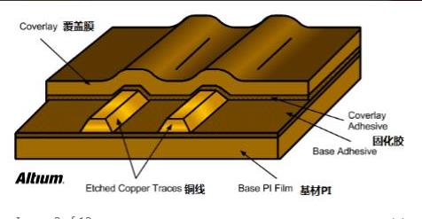
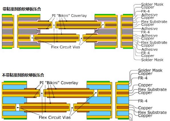
The trend of PCB design is to be light and thin. In addition to rigid flexible PCB, there are such important and complex fields as 3D connection and assembly of soft and hard boards. Soft and hard combination plate is also called rigid and flexible combination plate. With the birth and development of FPC, rigid flexible PCB (soft hard PCB), a new product, is gradually widely used in various occasions. Therefore, the soft and hard combination board is a circuit board with FPC characteristics and PCB characteristics formed by combining the rigid flexible PCB and the traditional hard circuit board according to the relevant process requirements through many processes. It can be used in some products with special requirements, including certain flexible areas and certain rigid areas.
The rigid flexible PCB is much more complex than the traditional PCB design in terms of design, and there are also many places to pay attention to. In particular, the rigid flexible PCBtransition area, as well as the relevant routing, through-hole and other aspects of design, need to follow the requirements of the corresponding design rules.

1. Through hole position
In dynamic use, especially when the soft plate is often bent, the vias on the soft plate should be avoided as much as possible. These vias are easy to be damaged and cracked. However, holes can be punched in the strengthening area of the soft board, but the edge line of the strengthening area should also be avoided. Therefore, in the design of soft and hard combination plates, a certain distance from the combination area should be avoided when drilling. As shown in the figure below.
2. Design of pad and via
When the pads and vias meet the electrical requirements, the maximum value shall be obtained. Smooth transition lines shall be used at the connection between pads and conductors to avoid right angles. The independent bonding pad shall be provided with a pad toe to strengthen the supporting effect.
Application of rigid flexible PCB Board in PCB Design. In the design of soft and hard combination plates, vias or pads are easily damaged. Rules to follow to reduce this risk:The larger the copper ring exposed on the soldering pad or via, the better. Try to add tears to the via wiring to increase the mechanical support. Add toe for reinforcement.
3. Routing design
If there are lines on different layers in the Flex area, try to avoid that one line is on the top layer and the other line is in the same path on the bottom layer. In this way, when the soft board is bent, the stress of the upper and lower layers of copper wire sheet is inconsistent, which is easy to cause mechanical damage to the line. Instead, they should be staggered and the paths should be arranged crosswise. As shown in the figure below.
4. Copper laying design
For flexible bending of reinforced flexible plates, it is better to adopt reticular structure for copper laying or plane layer. However, for impedance control or other applications, the electrical quality of the reticulated structure is unsatisfactory. Therefore, the designer needs to make a reasonable judgment on whether to use reticulated copper sheet or solid copper according to the design requirements. However, for the waste area, as much solid copper paving should be designed as possible.
5. Distance between drilling hole and copper sheet
This distance refers to the distance between a hole and the copper sheet, which is called "hole copper distance". The soft plate material is different from the hard plate material so it is difficult to deal with the too tight hole copper distance. Generally speaking, the standard hole copper spacing should be 10mil.

For the rigid flexible joint area, the two most important distances must not be ignored. One is the "Drill to Copper" mentioned here, which follows the minimum standard of 10mil. The other is the distance from the hole to the edge of the soft board (Hole to Flex), which is generally recommended to be 50mil.
6. Design of rigid flexible PCB joint area
In the rigid flexible joint area, it is better to design the FPC board to connect with the PCB board in the middle of the stack. The vias of soft plates are considered as buried holes in the rigid flexible joint area. Attention shall be paid to the rigid flexible joint area as follows:
The line shall be transited smoothly, and the direction of the line shall be perpendicular to the bending direction. The conductors shall be evenly distributed throughout the bend area. The width of the conductor shall be maximized throughout the bend area.PTH design shall not be adopted for rigid deflection transition zone.
7. Bending radius of bending area of rigid flexible PCB
The flexible bending area of rigid flexible PCB shall be able to withstand 100000 times of bending without open circuits, short circuits, performance degradation or unacceptable delamination. The bending resistance shall be measured by special equipment or equivalent instrument, and the tested sample shall meet the requirements of relevant technical specifications. In design, the bending radius should be shown in the figure below for reference.
The design of bending radius should be related to the thickness and number of layers of soft plates in the flexible bending area. The simple reference standard is R=WxT. T is the total thickness of soft plate. The single panel W is 6, the double-sided panel 12, and the multilayer panel 24. Therefore, the minimum bending radius of single panel is 6 times the thickness of the plate, double panel is 12 times the thickness of the plate, and multi-layer panel is 24 times the thickness of the plate. All shall be no less than 1.6mm. In a word, the design of rigid flexible PCB is particularly important for the design of soft and hard combination boards. During the design of flexible board, it is required to consider the different materials, thicknesses and combinations of the base material, adhesive layer, copper foil, covering layer and reinforcing plate of the flexible board, as well as the surface treatment, as well as its performance, such as peel strength, flexural resistance, chemical performance, working temperature, etc. Special consideration shall be given to the assembly and specific application of the designed flex board. The design rules in this regard can refer to IPC standards: IPC-D-249 and IPC-2233.
In addition, for the rigid flexible PCB processing precision of soft plate, the processing precision abroad: line width: 50 μ m. Aperture: 0.1mm, with more than 10 layers. Domestic: line width: 75 μ m. Aperture: 0.2mm, 4 layers. These rigid flexible PCB need to be understood and referred to in the specific design.