The detail of conformal coating
What is conformal coating?
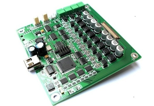
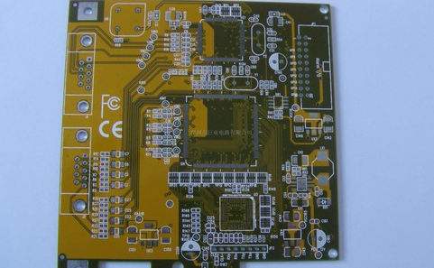
Conformal coating is a specially formulated coating used to protect Printed Circuit Board s and related equipment from environmental erosion. Conformal coating has good high and low temperature resistance; After curing, it forms a layer of transparent protective film, which has superior properties such as insulation, moisture-proof, anti leakage, shockproof, dust-proof, anti-corrosion, anti-aging, corona resistance and so on.
Under realistic conditions, such as chemical, vibration, high dust, salt fog, humidity and high temperature, the circuit board may have problems such as corrosion, softening, deformation and mildew, resulting in circuit failure of the circuit board.
The conformal coating is applied to the surface of the circuit board to form a layer of three proofing protective film (conformal coating refers to moisture-proof, salt fog proof and mildew proof).
Under the conditions of chemical substances (such as fuel, coolant, etc.), vibration, moisture, salt spray, humidity and high temperature, the circuit board without Electrical Insulating Varnish may be corroded, mold growth and short circuit, resulting in circuit failure. The use of conformal coating can protect the circuit from damage, so as to improve the reliability of the Printed Circuit Board and increase its safety factor, And ensure its service life.
In addition, since the conformal coating can prevent electric leakage, higher power and closer printed board spacing are allowed. Thus, the purpose of component miniaturization can be met.

Specifications and requirements for conformal coating process
Painting requirements:
1. Painting thickness: the thickness of paint film shall be controlled within 0.05mm-0.15mm. The dry film thickness is 25um-40um.
2. Secondary coating: in order to ensure the thickness of products with high protection requirements, secondary coating can be carried out after the paint film is cured (whether to carry out secondary coating is determined according to the demand).
3. Inspection and repair: visually inspect whether the coated circuit board meets the quality requirements, and repair the problems. For example, if the pins and other protected areas are stained with three proofing paint, they can be scrubbed with tweezers holding degreasing cotton balls or clean cotton balls dipped in board washing water. During scrubbing, pay attention not to wash off the normal paint film.
4. Component replacement: after the paint film is cured, if you want to replace the component device, you can do the following:
(1) Solder down the components directly with electric ferrochrome, and then clean the materials around the pad with cotton cloth dipped in board washing water
(2) Welding alternative components
(3) The welding part shall be coated with a solid brush dipped in the three proofing paint brush, and the surface of the paint film shall be dry and solidified
Operation requirements:
1. The three anti paint workplace shall be clean and free of dust. Good ventilation measures must be taken, and irrelevant personnel are prohibited from entering.
2. Wear respirators or gas masks, rubber gloves, chemical protective glasses and other protective equipment during operation to avoid injury to the body.
3. After the work is completed, the used tools shall be cleaned in time, and the 2 devices equipped with three proofing paint shall be closed and tightly covered.
4. Anti static measures shall be taken for the Printed Circuit Board. The circuit board shall not be overlapped. During the coating process, the circuit board shall be placed horizontally.
Quality requirements:
1. The surface of the circuit board shall be free of paint flow and leakage. When painting with the brush, pay attention not to drip to the locally isolated part.
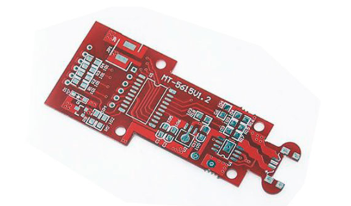
2. The conformal coating layer shall be flat, bright and uniform in thickness, and the surface of pad, patch element or conductor shall be well protected.
3. There shall be no bubbles, pinholes, corrugations, shrinkage cavities, dust and other defects and foreign objects on the surface and components of the paint layer, and there shall be no pulverization and peeling. Note: the paint film shall not be touched at will before the paint film is dry.
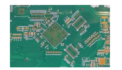
4. Locally isolated elements or areas shall not be coated with conformal coating.
Parts and devices that cannot be coated with conformal coating
1. Conventional uncoated devices: paint high-power radiator, heat sink, power resistance, high-power diode, cement resistance, code pulling switch, potentiometer (adjustable resistance), buzzer, battery base, fuse base, IC base, touch switch, relay and other types of sockets, pins, wiring terminals and DB9, plug-in or patch LED (non indicating function), nixie tube, Ground screw hole.
2. Parts and devices that cannot use conformal coating specified by the drawing.
3. According to the detailed provisions in the catalogue of non conformal coating components (areas),conformal coating shall not be used.
If the conventional uncoated devices in the regulations need to be coated, the R & D department can specify the requirements or the drawings can carry out three anti coating.
Precautions for conformal coating spraying process
1. PCBA must be provided with process edge and the width shall not be less than 5mm, which is convenient for getting on the machine and walking the track.
2. The maximum length and width of PCBA board is 410 * 410mm and the minimum is 10 * 10mm.
3. The maximum height of PCBA mounted components is 80mm.
4. The minimum distance between the spraying area and the non spraying area of the components on PCBA is 3mm.
5. Thorough cleaning can ensure that the corrosive residues are completely removed and the three anti paint is well adhered to the surface of the Printed Circuit Board. The paint thickness should be between 0.1-0.3mm. Drying conditions: 60 ° C, 10-20 minutes.
6. In the process of spraying, some components can not be sprayed, such as high-power components with heat dissipation surface or radiator, power resistance, power diode, cement resistance, dial switch, adjustable resistance, buzzer, battery base, fuse base (tube), IC base, light touch switch, etc.
Introduction to repair of conformal coating for Printed Circuit Board
When the circuit board needs to be repaired, the expensive components on the circuit board can be taken out separately and the rest can be discarded. But the more common method is to remove the protective film at all or local positions on the printed circuit board and replace the damaged components one by one.
When removing the conformal coating protective film, ensure that the substrate under the components, other electronic components, structures near the repair position, etc. will not be damaged. The removal methods of protective film mainly include the use of chemical solvent, micro grinding, mechanical method and disassembly and welding through protective film.
Using chemical solvent is the most commonly used method to remove the tconformal coating protective film. Its key lies in the chemical properties of the protective film to be removed and the chemical properties of the specific solvent.
Micro grinding uses the high-speed particles ejected from the nozzle to "grind" the three anti paint protective film on the Printed Circuit Board.