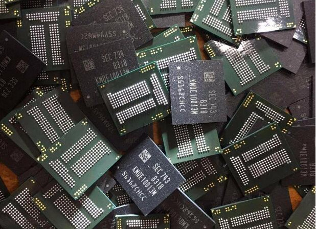
We all know that when there are only a few samples, manual soldering can be used, while batch PCBA processing requires PCBA assembly production lines. So what equipment will be used in the PCBA assembly line?
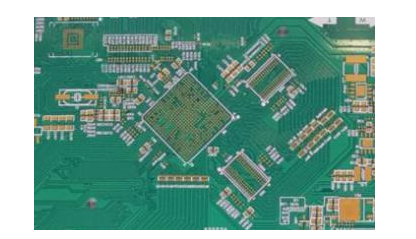
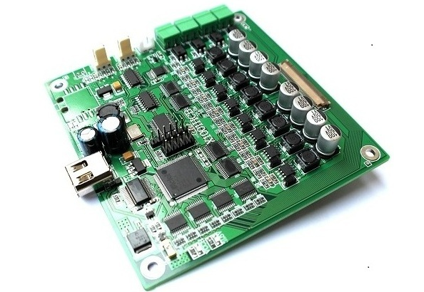
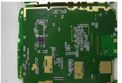
In PCBA assembly, there are 4 main stages of SMT or surface mount technology assembly using reflow soldering, that is, setting up the mounting application, automatic component placement, soldering and inspection (and testing if necessary). The basic equipment required for PCBA assembly includes:
1. Solder Paste Printer
2. Solder Paste Inspection (SPI) Machine
3. Dispenser
4. Mounter
5. Reflow soldering machine
6. Wave soldering machine (for through-hole components)
7. Automatic optical inspection (AOI) machine
8. Online test (ICT) fixture
9. Functional verification test (FVT) device
Phase 1: Placement application
1. Solder Paste Printer
The first step in PCBA assembly is to apply solder paste to the board. Solder paste is a gray glue made from a mixture of tiny metal alloys. Usually tin, lead and silver. Think of it as the glue that holds the finished circuit board together. Without it, the components will not stick to the bare board.

Before applying the paste, place the PCB template on the board. The PCB template is a stainless steel plate with small laser-cut holes. These fluxes can only be applied to the component to contact the circuit board area that will eventually be located on the finished PCB, that is, the SMD pad.
During the solder paste application, the PCB template and PCB are locked in place in the automatic solder paste printer. Then, the squeegee spreads the lead-free solder paste on the pad in a precise amount. Then, the machine drags the blade on the template to spread the paste evenly and deposit it in the desired area. After removing the template, the solder paste will be exactly where we want it (hopefully).
2. Solder Paste Inspection (SPI) Machine
Numerous industry studies have pointed out that up to 70% of SMD soldering problems can be traced to incorrect or unqualified solder paste printing. Therefore, the next step is to check whether the solder paste is correctly printed on the board. Although a good solder paste printing method is usually sufficient to meet the needs of small batches of PCBs, SPI should be considered when producing large numbers of PCBs in batches to avoid higher rework costs.
The SPI machine uses a camera capable of capturing 3D images to evaluate the quality of solder paste based on factors such as solder volume, alignment, and height. Then, the machine can quickly identify the inappropriate amount of solder or incorrect alignment, so that the manufacturer can quickly find the bad solder paste printing and correct the problem. When used with automatic optical inspection (described in detail later), this allows manufacturers to effectively monitor and control the solder printing process, thereby reducing rework costs and producing high-quality PCBs more efficiently.
Phase 2: Automated component placement
3. Dispenser
Before placing the component, the dispenser applies glue dots to the PCB where the component body will be placed to fix it in place until the leads and contacts are soldered. This is very important for wave soldering. In wave soldering, the wave crest may remove larger components, or for double-sided wave soldering or reflow soldering to prevent components from falling.
4. Mounter
The placement machine is probably the most fascinating machine in the entire assembly line. As the name suggests, the pick-and-place machine picks up the components and places them on the bare board. Traditionally, this stage of the PCBA assembly process is done by hand. At this stage, people use tweezers to pick and place components laboriously. Fortunately, today's PCB manufacturers have used pick and place machines to automate this step, because machines are more accurate than humans and can work around the clock.
The placement machine picks up SMT components and places them accurately at the pre-programmed position on top of the solder paste. They fell at lightning speed, and the machine easily reached a speed of 30,000 parts per hour. Since the machine places parts in an orderly but almost crazy way, watching and placing the machine's work is undoubtedly the most interesting viewing!
The third stage: welding
5. Reflow soldering machine
Reflow soldering is the most widely used soldering technique in PCBA assembly. Once the board is fully loaded with components, the components move along a conveyor belt through a long giant oven (called a reflow soldering machine). The PCB board passes through various areas at a strictly controlled temperature to make the solder paste melt and harden stably, thereby forming a strong electrical connection between the components and their respective pads.
6. Wave soldering machine
The wave soldering machine got its name because the PCB must pass through a wave of molten solder to solder the components. At the beginning of the wave soldering process, a so-called flux layer is applied to clean all component contacts and pads to ensure proper solder adhesion. After the flux is applied, the board is preheated to prevent thermal shock. Finally, a solder wave is established in the molten solder pot, and then the PCB is passed through, bringing the underside of the board into contact with the solder wave, thereby forming a connection between the leads of the components or their respective holes and contacts of the leads. Pads.
However, compared with reflow soldering, wave soldering is not widely used in today's PCBA assembly because the latter is much more effective in soldering the fine features of the boards with surface mount components used today. As a result, wave soldering and more recently selective wave soldering methods are used to assemble through-hole components.
Phase 4: Inspection
7. Automated Optical Inspection (AOI)
Now that the circuit board is fully assembled, it can now be inspected and tested. As the complexity of PCB boards increases, automatic optical inspection is more important than ever. Although you can still squint and spot errors with the naked eye, manual inspection is not effective at mass production because the operator will quickly become tired and errors can easily be ignored. Testing PCBA is a key step in PCBA manufacturing to avoid expensive remanufacturing costs and material waste. The AOI system is used to detect problems early in the production process and allows modification of the process or correction of individual boards.
Using optical methods to detect defects, AOI systems can perform inspections previously done by humans, but with much higher speed and accuracy. The AOI machine uses a high-definition camera to capture the surface of the circuit board and build an image for analysis. The captured image is then compared with the image of the correct reference board to identify various defects, from incorrect and missing components to short circuits and scratches.
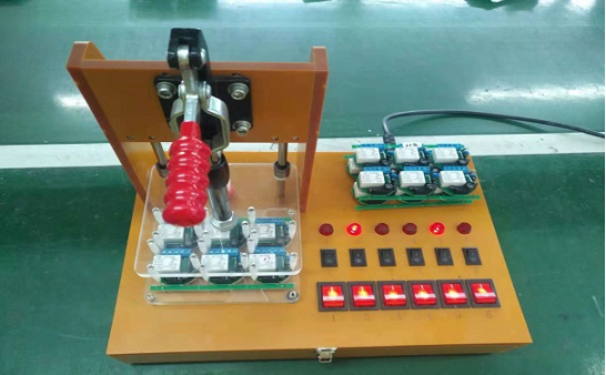
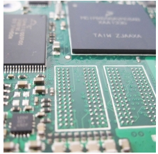
8. Online Test (ICT)-Nail Bed
The in-line test (ICT) stage is carried out using a nail clipper fixture, which is one of the most widely recognized methods for quickly testing the function of the assembled PCB board. Due to the unusual similarity of the test bench to the torture device, named after the real nail bed, the test fixture consists of a series of spring-loaded pogo pins arranged so that each pin is in contact with a node in the PCB circuit. Each completed circuit board is placed on top of these pins and pressed down to quickly establish contact through hundreds of test points on the PCB. Through these test points, the fixture can quickly transfer test signals to and from the PCB to evaluate its performance and detect electrical continuity or short circuit interruptions.
PCBA tested on the nail bed may be evidenced by the small dents seen on the solder connection due to the sharp tip of the pin. Therefore, when your PCBA has small dents, don't panic! This is a cause for celebration, because it shows that your manufacturer has properly tested to ensure that your circuit board is intact.
9. Functional Verification Test (FVT)
The functional verification test (FVT) is the final step, which can provide a pass or fail decision for the completed PCB before shipment. By this time, we are no longer just testing physical defects, such as solder bridges or tombstones. Instead, the software is loaded and we are testing whether the board will work properly when used in any application the customer wants.
FVT usually simulates the operating environment in which the PCB will eventually be used by connecting the PCB to the PCB through its connectors or test points. Functional testing varies from product to product, because each tested PCB is unique. The most common form of functional testing is the "thermal model", which is a configuration used to simulate the final product in which the PCB will be used. However, no matter how to customize FVT, they all share a common component. System, hardware and software.