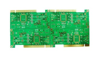
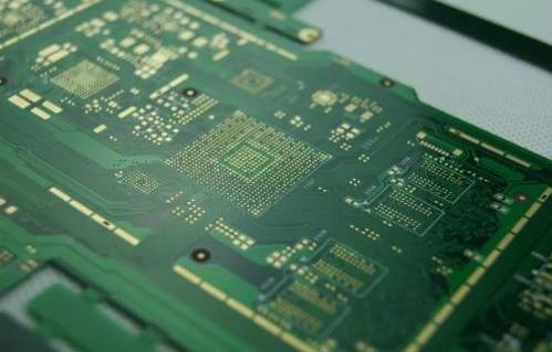
PCBA processing is based on the production materials produced by PCB design. Excellent PCB design will facilitate subsequent PCBA processing, and imperfect design will affect the processing process and even affect the quality of the product. So what are the PCB design factors that will affect PCBA processing?
PCB design factors that affect PCBA processing:
1. The upper tin position cannot have a silk screen image.
2. The minimum distance between the copper foil and the board edge is 0.5mm, and the minimum distance between the component and the board edge is 5.0mm. The minimum distance between the pad and the board edge is 4.0mm.
3. The minimum gap of copper foil: 0.3mm for single panel and 0.2mm for double panel.
4. When designing the double panel, pay attention to the components of the metal shell. When the shell is in contact with the printed board when plug-in, the top pad cannot be opened, and it must be covered with solder mask oil or silk screen oil.

5. Do not place jumpers under the IC or under the components of motors, potentiometers and other large-volume metal casings.
6. Electrolytic capacitors should not touch heating components. Such as high-power resistors, thermistors, transformers, radiators. The minimum distance between the electrolytic capacitor and the radiator is 10mm. The distance between other components and the radiator is 2.0mm.
7. Large-scale components (such as transformers, electrolytic capacitors with a diameter of 15mm or more, high-current sockets.) should increase the pad.
8. The minimum line width of copper foil: 0.3mm for single-sided boards, and at least 1.0mm for the copper foil on the 0.2mm side of double-sided boards.
9. There should be no copper foil (except for grounding) and components (or as required by the structure drawing) within 5mm of the screw hole radius.
10. The pad size (diameter) of the general through-hole mounting component is twice the aperture. The minimum size of the double-sided board is 1.5mm, and the minimum size of the single-sided board is 2.0mm.
11. If the distance between the center of the pad is less than 2.5mm, the adjacent pads must be wrapped with silkscreen oil, and the width of the silkscreen oil is 0.2mm.
12. Components that need to be soldered after soldering through a soldering furnace. The soldering pads should be driven away from the tin position. The direction is opposite to the soldering direction. It is 0.5mm to 1.0mm. This is mainly used for single-sided mid-post soldered soldering pads to avoid soldering. Time blocked.
13. In the large-area PCB design (approximately more than 500cm), in order to prevent the PCB board from bending when going through the tin furnace, a gap of 5mm to 10mm should be left in the middle of the PCB board without placing the components (wires can be routed) to be used in the process. Add bead to prevent bending when tin furnace.
14. In order to reduce the short-circuit of the solder joints, all double-sided boards and vias do not open solder mask windows.
The above is an introduction to the PCB design factors that affect PCBA processing. I hope it will be helpful to everyone.