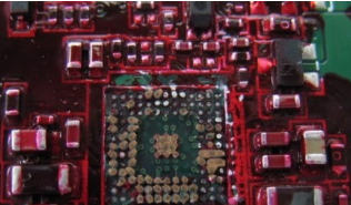
If you are a PCBA engineer, then you must have used X-Ray and used it to see the soldering conditions of BGA, but how do you think the BGA balls look the same? How do you judge BGA Is there any empty welding?
Generally speaking, most people using X-Ray can only see if the solder has shorts, less solder, and voids, but it is a bit difficult to judge whether the BGA balls are free to solder. Of course, this refers to the 2D X-Ray, in fact, if you are more careful, you can still find a little clue to determine whether there is free soldering!
Generally speaking, the images taken by X-Ray are only simple 2D projection images. It is easy to use it to check short circuits (shorts), but it is difficult for many people to use it to check empty soldering, because every BGA solder ball It looks almost round, and it is hard to tell whether there is any empty welding. Although there has been a [3D X-Ray CT] that claims to be able to take 3D images in recent years, it costs a lot! And whether it can be as magical as the business claims, I really dare not dream.
Here is how to use the traditional 2D planar X-Ray image to determine whether the BGA is empty.
1. BGA solder balls become larger and cause empty soldering

First of all, think about the same size of the solder balls of the same BGA. If some of the solder balls are empty and some are intact, will the two types of solder have different shapes? The answer is yes. Imagine that after a solder ball of the same volume is compressed, a part of the solder ball of good solder will disperse to the PCB pad and make the solder ball smaller; the solder ball with free soldering will not, The solder ball will become bigger after being compressed.
The following figure shows that the diameter of the solder ball will become larger when the solder ball of the same size is empty. Of course, it is better to compare whether the solder balls of the normal board are all the same size, because the design of some boards will cause the solder ball to become smaller., Will be detailed later.
When a solder ball of the same size of BGA is soldered, the diameter of the solder ball will increase instead.
When a solder ball of the same size of BGA is soldered, the diameter of the solder ball will increase instead.
In addition, Shenzhen Honglijie also believes that this phenomenon of solder ball enlargement has a very high positive correlation with HIP (Head In Pillow) and NWO (Non-Wet-Open) bad phenomena. However, both HIP and NWO are generally It is difficult to check it with two-dimensional (2D) X-Ray, because the size of the BGA sphere does not change much.
2. Vias lead to empty soldering with insufficient tin
Another phenomenon of PCB empty soldering is insufficient tin. This phenomenon usually occurs when the solder pad has vias, because part of the tin will be caused by the wicking phenomenon when the solder ball flows through the reflow. ) Insufficient amount of tin caused by flowing into the via hole. Sometimes the via hole next to the solder pad can also cause such a problem. At this time, the sphere seen from the X-Ray will become smaller, and the amount of tin is eaten by the via hole, and the solder will be empty. Generally, we don't recommend making vias on the solder pads. The vias next to the solder pads should also be covered with green paint (solder mask). The shortcomings and remedies of via in pads will be discussed later.
▼This is a poor design with the vias placed next to the solder pads. In this design, the solder is very easy to flow into the through holes and cause the phenomenon of empty soldering due to insufficient tin.
This is a poor design with the vias placed next to the solder pads. This design solder is very easy to flow into the vias, resulting in an insufficient amount of solder.
Three, there are air bubbles in the solder ball to produce empty solder
Another reason for the formation of BGA empty soldering is that there are voids in the solder ball. According to the IPC7095 7.4.1.6 specification, the general PCB electronics industry is suitable for Class 1. The total hole diameter of all the bubbles cannot exceed the BGA diameter. 60% of it. If the bubbles are too large, it will cause empty soldering or solder cracking. (Correction on 2010/11/22, general electronic products should be applied to Class 1 instead of Class 3, and additional explanations of various levels are added)
Class 1: Suitable for general consumer electronic products. The bubble requirement of BGA should not be greater than 60% (diameter) or 36% (area).
Class 2: Suitable for commercial/industrial electronic products. The bubble requirement of BGA should not be greater than 42% (diameter) or 20.25% (area).
Class 3: Suitable for military/medical electronic products. The bubble requirement of BGA should not be greater than 30% (diameter) or 9% (area).
2012-Jul-01 update: According to the IPC-7095B 7.5.1.7 specification update, the air bubbles in the BGA solder ball are now uniformly required to be no more than 25% (diameter) or 6.25% (area).