COB (Chip On Board) is already a mature technology in the PCB manufacturing industry, but the general PCBA assembly factory is not familiar with its process, perhaps because it uses some wire bond integrated circuit (IC) packaging Technology, so it is difficult for many finished products or professional PCB foundries to find relevant technical personnel.
In the past, COB was mostly only used in some low-end consumer products. As electronic products became smaller and smaller, more and more companies began to consider introducing COB processes into their products. After all, the space available on the circuit board An inch of land and an inch of gold, and the COB process can use a space smaller than that of an IC. Perhaps it is too expensive to adopt more advanced technology, so some people come back to consider the COB process.
Here I will reorganize the experience of setting up and operating COB many years ago. On the one hand, I remind myself of this process, and on the other hand, I provide reference. Of course, some information may not be up-to-date and is for reference only.

Understand the evolution history of electronic chip packaging. From IC packaging - COB - Flip Chip (COG), the size is getting smaller and smaller. Among them, COB can only be said to be an intermediate product between the current technology. In addition, CSP (Chip Scare Package) should be a process between COB and Flip Chip! It's really messy.
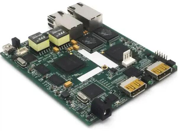
To put it bluntly, COB is just to transplant the IC package wire bonding and sealing (Caplu) operations to the circuit board, that is to say, change the bare wafer (die) originally attached to the leadframe. Paste on the circuit board (PCB), and re-solder the wires/wires that were originally bonded to the lead frame to the gold-plated pads of the PCB, and then use Epoxy to cover the wafers and wires to replace the original COB can save the original ICf package trimming & form (Triming&Form) and printing (marking) process, and it can also reduce the cost of IC packaging factory sales, so basically its process will be more than IC packaging process Cheap.
Because it is cheap, early COB technology is generally only used in low-level consumer electronic products that do not pay much attention to reliability, such as toys, calculators, small displays, clocks and other daily necessities, because these products are so cheap that you If it is worn out, throw it away and buy a new one. Therefore, in the early days of Taiwan's COB process, most of the COB processes were set up by the employees of IC packaging factories. The living room is the PCB factory, and there is no environmental control. It is often mistaken that the quality of COB is not reliable enough.
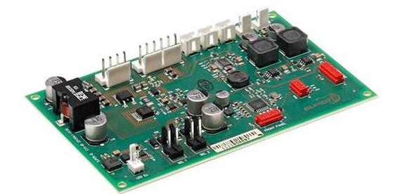
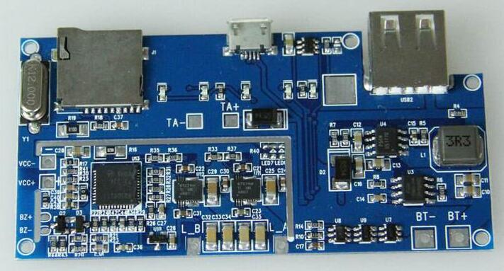
However, with the progress of the times, more and more large PCB manufacturers are interested in its small size, as well as the trend of lighter, thinner and shorter products. In recent years, the use of COB has become more and more popular, such as mobile phones, cameras and other requirements. Many of its products have been introduced into the COB process.
COB has another advantage that some manufacturers particularly love it. Due to the need for "sealing glue", the general COB will seal all the external wire pins in epoxy resin (Epoxy). For those hackers who like to crack other people's designs, they may need to spend more because of this feature. More time to crack, indirectly achieved the improvement of the anti-hacking security level. (※: The anti-hacking security level is determined by how much time and money it takes to crack a technology, the more time and money it takes, the higher the level)