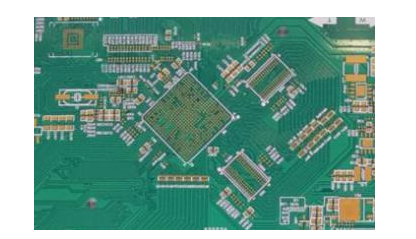
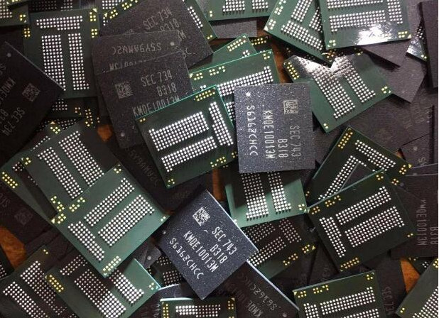
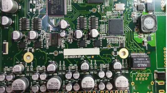
Most electrical equipment has PCBA inside. It is a magical board. The narrow board is filled with densely packed power electronic devices, helping the electronic equipment to complete various functions. So, what are the steps for PCBA in baking sheet processing? What are the common problems? Let's take a closer look at "Baking plate steps and common conditions of PCBA processing" below.
[What are the common conditions of PCBA processing]
In the PCB processing and welding process, the performance of the flux directly affects the quality of the welding. So what are the common welding defects of PCBA processing? How to analyze and improve the bad welding?
1. Bad condition: There are too many residues on the PCB board surface after welding, and the board is dirty.
Result analysis:
(1) The temperature of the tin furnace is not enough because it is not preheated before welding or the preheating temperature is too low;
(2) The walking speed is too fast;
(3) Anti-oxidant and anti-oxidant oil are added to the tin liquid;
(4) Too much flux coating;
(5) The component feet and the orifice plate are out of proportion (the holes are too large), which causes the flux to accumulate;
(6) During the use of flux, no thinner is added for a long time.

2. Bad condition: easy to catch fire
Result analysis:
(1) The wave furnace itself has no air knife, which causes the flux to accumulate and drip onto the heating tube during heating;
(2) The angle of the air knife is incorrect (uneven flux distribution);
(3) There is too much glue on the PCB and the glue is ignited;
(4) The board travel speed is too fast (the flux is not completely volatilized and drips onto the heating tube) or too slow (the board surface is too hot);
(5) Process problems (pcb sheet, or PCB is too close to the heating tube).
3. Bad condition: Corrosion (green components, black solder joints)
Result analysis:
(1) Insufficient preheating causes too many flux residues and too many harmful residues;
(2) Use the flux that needs cleaning, but there is no cleaning after soldering.
4. Bad condition: electric connection, leakage (poor insulation)
Result analysis:
(1) PCB design is unreasonable
(2) PCB solder mask is of poor quality and easy to conduct electricity
5. Unfavorable phenomena: virtual welding, continuous welding, missing welding
Result analysis:
(1) The amount of flux coating is too small or uneven;
(2) Some pads or solder feet are seriously oxidized;
(3) PCB wiring is unreasonable;
(4) The foaming tube is clogged and the foaming is uneven, resulting in uneven flux coating;
(5) Improper operation method when immersing tin by hand;
(6) The inclination of the chain is unreasonable;
(7) The wave crest is uneven.
6. Bad phenomenon: the solder joints are too bright or the solder joints are not bright
Result analysis:
(1) This problem can be solved by choosing bright or matt flux;
(2) The solder used is not good.
7. Undesirable phenomena: smoke and smell
Result analysis:
(1) The problem of the flux itself: the use of ordinary resin will cause more smoke; the activator has a lot of smoke and has a pungent odor;
(2) The exhaust system is not perfect.
8. Unfavorable phenomena: splashing, tin beads
Result analysis:
(1) Process: low preheating temperature (the flux solvent is not completely volatilized); the board travel speed is fast, and the preheating effect is not reached; the inclination of the chain is not good, there are bubbles between the tin liquid and the PCB, and tin beads are generated after the bubbles burst; Improper operation during immersion tin; humid working environment;
(2) The problem of PCB: the board surface is wet and moisture is generated; the design of the outgassing hole of the PCB is unreasonable, resulting in air trapping between the PCB and the tin liquid; the design of the PCB is unreasonable, and the parts feet are too dense to cause air trapping.
9. Bad phenomenon: poor soldering, insufficient solder joints
Result analysis:
(1) The double wave process is used, and the effective components of the flux have been completely volatilized when the tin is passed;
(2) The board walking speed is too slow and the preheating temperature is too high;
(3) Uneven flux coating;
(4) The pads and component feet are seriously oxidized, causing poor tin eating;
(5) There is too little flux coating to completely wet the pads and component pins;
(6) The PCB design is unreasonable, which affects the soldering of some components.
10. Bad phenomenon: PCB solder mask falls off, peels off or blisters
Result analysis:
(1) More than 80% of the reasons are problems in the PCB manufacturing process: poor cleaning, poor quality solder mask, PCB board and solder mask mismatch, etc.;
(2) The temperature of the tin liquid or the preheating temperature is too high;
(3) Too many welding times;
(4) The PCB stays on the surface of the tin liquid for too long during the manual tin immersion operation.
The above is the bad welding phenomenon and result analysis in the PCBA processing.
[Common sense of the baking sheet process of PCBA processing]
Before PCBA processing, there is a process that many PCBA manufacturers will ignore, and that is the baking sheet. The baking sheet can remove the moisture on the PCB board and the components, and after the PCB reaches a certain temperature, the flux can better bond with the components and the pads. The welding effect will also be greatly improved. Let me introduce you to the baking sheet process in PCBA processing.
1. Instructions for PCBA processing baking sheet:
1. PCB board baking requirements: the temperature is 120±5 degree Celsius, generally bake for 2 hours, and start timing when the temperature reaches the baking temperature. Specific parameters can refer to the corresponding PCB baking specifications.
2. PCB baking temperature and time setting
(1) PCB sealed and unpacked within 2 months of manufacture date for more than 5 days, bake at 120±5 degree Celsius for 1 hour;
(2) PCBs with a manufacturing date of 2 to 6 months, bake at a temperature of 120±5°C for 2 hours;
(4) PCBs with a manufacturing date between 6 months and 1 year, baked at a temperature of 120±5°C for 4 hours;
(5) PCBs that have been baked must be processed within 5 days, and unprocessed PCBs need to be baked for another hour before they can go online;
(6) PCBs older than one year from the manufacturing date can be baked at 120±5°C for 4 hours and re-sprayed with tin to go online.
3. PCBA processing and baking method
(1) Large PCBs are mostly placed in a flat style, with 30 more stacked, and the PCB is taken out of the oven within 10 minutes after the baking is completed, and placed flat at room temperature to cool down naturally.
(2) Small and medium-sized PCBs are mostly placed horizontally, with more than 40 pieces stacked, and the number of vertical types is not limited. Take out the PCB from the oven within 10 minutes after baking, and place it flat at room temperature to cool down naturally.
4. The components that are no longer used after repairing do not need to be baked.
2. PCB baking requirements:
1. Regularly check whether the material storage environment is within the specified range.
2. The staff must be trained.
3. If there is any abnormality in the baking process, the relevant technical personnel must be notified in time.
4. Anti-static and heat insulation measures must be taken when touching materials.
5. Leaded materials and lead-free materials need to be stored and baked separately.
6. After baking, it must be cooled to room temperature before it can be put on line or packaged.
Three, PCBA baking precautions:
1. When the skin touches the PCB board, you must wear heat-insulating gloves.
2. The baking time must be strictly controlled, not too long or too short.
3. The baked PCB board must be cooled to room temperature before going online.