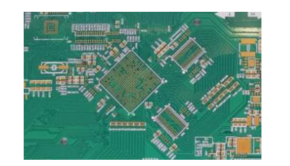
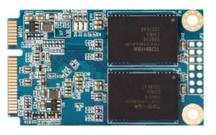
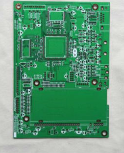
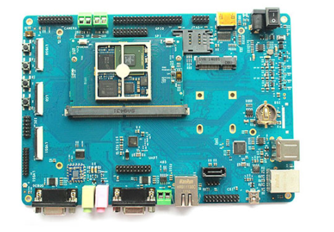
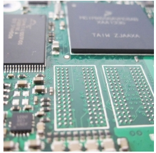
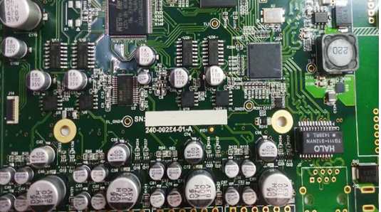
PCBA processing printed board graphic production link control
Paying attention to the trend of environmental protection informatization and the development of various environmental protection technologies, PCB factories can start with big data to monitor the company's pollution discharge and governance results, and find and solve environmental pollution problems in a timely manner. Keep up with the production concept of the new era, continuously improve resource utilization, and realize green production. Strive to make the PCB factory industry realize an efficient, economical and environmentally friendly production model, and actively respond to the country's environmental protection policy.
2. The influence of PCBA processing silk screen on the quality of graphics transfer
The surface of the copper clad laminate must be pre-treated before the graphics transfer to ensure that the ink silk screen layer and the copper foil have a good bonding force. Usually use mechanical/chemical combined processing grinding plate production line to remove the oxide layer and impurities on the surface of the plate. The control of the printing thickness and pre-bake time of the screen printing photosensitive film is the key to the control of this link.
The thickness of the screen printing of general liquid resist photosensitive ink (commonly known as wet film) is determined by the number of screen meshes selected. According to processing experience, the screen printing mesh number is 120 mesh to 160 mesh, and the hardness of the squeegee is 700-750 for silk printing, and the effect is better. The process of pre-baking after screen printing is controlled strictly according to the process parameters. The silk-screen printing environment requires dust-free, to prevent dust and debris from falling into the silk-screen board, affecting the quality of fine graphics.
The boards that are dirty on the screen surface, the ink enters the holes, and the pre-bake is over or under-bake are all processed for unwashing. For the board that has just been silk-screened and pre-baked, it should be allowed to stand for 10min-15min before moving to the next process.

3. The influence of PCBA processing exposure and development on the quality of graphics transfer
The graphics transfer of the printed board is really realized through the exposure and development process.
The exposure process first controls the cleanliness of the environment, the cleaning of the exposure machine, and the cleaning of the workbench (according to the specified cleaning frequency). Regularly check and clean the film master, exposure machine, and table surface during the exposure process. Correct and repair the problems found in the inspection process in time.
Graphics transfer must also strictly control the exposure parameters and the accuracy of the alignment. The parameter control of exposure energy, time, etc., is strictly implemented according to the process parameters. The board transferred from the silk screen must be cooled to room temperature before exposure, and after the printed board is exposed, let it stand for more than 15 minutes before developing. At the same time, pay attention to the influence of developing syrup, temperature, effect and other links on graphics transfer.
The last part of PCBA processing graphics transfer is the board repair inspection, that is, the correctness and completeness of the graphics are comprehensively checked, and the board is repaired to the deficiencies. Focus on checking the graphics circuit for potential defects that may cause disconnection gaps; check whether the wet film layer has exposed copper or pinholes; whether there are partial holes or film drop; check the development quality of the graphics circuit, whether the lines have broken lines or lines Please wait for the problem, wash the unqualified board back and do it again.
Our factory is located in China. For decades, Shenzhen has been known as the world's electronics R&D and manufacturing center. Our factory and website are approved by the Chinese government, so you can skip the middlemen and buy products on our website with confidence. Because we are a direct factory, this is the reason why 100% of our old customers continue to purchase on iPCB.