One, the solution to the solder ball produced by SMT reflow soldering
(1) The principle of solder ball formation in reflow soldering:
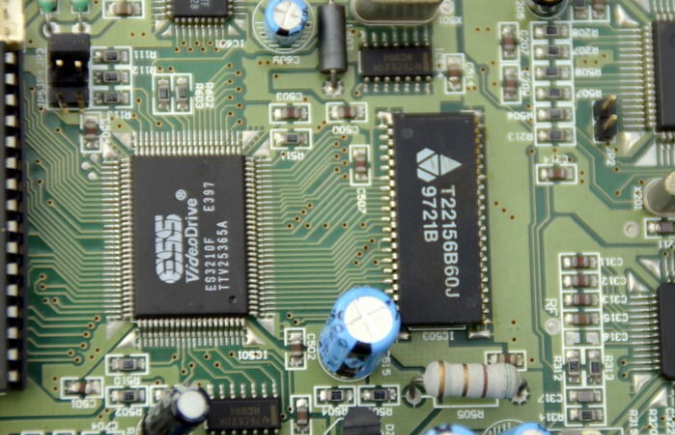
The solder balls produced during reflow soldering are often hidden in the sides or between the fine pitch pins between the two ends of the rectangular chip component. During the component mounting process, the solder paste is placed between the pins and the pads of the chip components. As the printed board passes through the reflow oven, the solder paste melts and becomes liquid. If the wetting is not good, the liquid solder will shrink and make the welding seam insufficiently filled, and all the solder particles cannot aggregate into a solder joint. Part of the liquid solder will flow out of the solder joints and form solder balls. Therefore, poor wettability of solder with pads and device pins is the root cause of the formation of solder balls.
(2) The following mainly analyzes the causes and solutions related to related processes:
1. Improper setting of reflux temperature curve. The reflow of solder paste is a function of temperature and time. If it does not reach a sufficient temperature or time, the solder paste will not reflow. The temperature rise in the preheating zone is too fast, and the time to reach the top temperature is too short, so that the moisture and solvent in the solder paste are not completely volatilized. When it reaches the reflow soldering temperature zone, the moisture and solvent will boil and the solder balls will be splashed. Practice has proved that it is ideal to control the temperature rise rate of the preheating zone at 1~4°C/s.
2. If solder balls always appear in the same position, it is necessary to check the metal plate design structure.

The corrosion accuracy of the template opening size cannot meet the requirements. For the PCB pad size is too large, and the surface material is soft (such as copper template), the outline of the missing solder paste is not clear and bridges each other. This situation often occurs in When the pads of fine-pitch devices are missed, a large number of tin beads between the pins will inevitably be produced after reflow soldering. Therefore, according to the different shapes and center distances of the pad patterns, appropriate template materials and template manufacturing processes should be selected to ensure the quality of solder paste printing.
3. If the time from mounting to reflow soldering is too long, due to the oxidation of the solder particles in the solder paste, the flux will deteriorate and its activity will decrease, which will cause the solder paste to not reflow and solder balls will be produced. Choosing a solder paste with a longer working life (at least 4 hours) will reduce this effect.
4. In addition, the printed board with the wrong solder paste is not cleaned sufficiently, leaving the solder paste on the surface of the printed board and through holes. Before reflow soldering, the placed components are realigned and placed to deform the missing solder paste. These are also the causes of solder balls. Therefore, it is necessary to strengthen the sense of responsibility of operators and process personnel in the production process, strictly follow the process requirements and operating procedures for production, and strengthen the quality control of the process.
Second, the solution to the tombstone caused by SMT reflow soldering
(1) The principle of the formation of the reflow soldering neutral sheet:
One end of the rectangular chip component is soldered to the pad, while the other end is upright. This phenomenon is called the Manhattan phenomenon. The main cause of this phenomenon is that the two ends of the component are not heated uniformly, and the solder paste is melted sequentially.
(2) How to cause uneven heat at both ends of the PCB component:
1. Defective component arrangement direction design.
We imagine that there is a reflow limit line that spans the width of the furnace in the reflow soldering furnace, which will melt as soon as the solder paste passes through it. One end of the chip rectangular component passes through the solder limit line first, and then the solder paste is melted first, and completely wets the metal surface of the component, with liquid surface tension; while the other end does not reach the liquid phase temperature of 183°C, the solder paste is not melted. There is only the adhesive force of the flux, which is much smaller than the surface tension of the reflowed solder paste, so that the component end of the unmelted end is upright. Therefore, keep the two ends of the component entering the reflow solder limit line at the same time, so that the solder paste on the pads at both ends will melt at the same time, forming a balanced liquid surface tension, and keeping the component position unchanged.
2. Insufficient preheating of printed circuit components during vapor phase welding.
Vapor phase soldering uses inert liquid vapor to condense on the component pins and PCB pads to release heat to melt the solder paste. Vapor phase welding is divided into balance zone and saturated steam zone. The welding temperature in the saturated steam zone is as high as 217°C. During the production process, we found that if the welded component is not fully preheated and undergoes a temperature difference of more than 100 degrees, vapor phase welding The evaporating force easily floats the chip components smaller than the 1206 package size, resulting in a stand-up phenomenon. We preheat the component to be welded in the high and low box at a temperature of 145°C-150°C for 1-2 minutes, then preheat it in the equilibrium zone of vapor phase welding for about 1 minute, and finally slowly enter the saturated vapor zone for welding Eliminates the phenomenon of standing films.
3. The influence of PCB pad design quality.
If the size of a pair of pads of a chip component is different or asymmetric, it will also cause inconsistencies in the amount of missing solder paste. Small pads respond quickly to temperature, and the solder paste on them is easy to melt, while large pads are the opposite. Therefore, When the solder paste on the small pad is melted, the component is straightened up under the action of the surface tension of the solder paste. If the width or gap of the pad is too large, the phenomenon of standing up may also appear. Strictly following the standard specification for the design of the pad is a prerequisite for solving this defect.