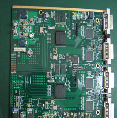
In the SMT patch, the patch inductor is mainly responsible for choking, decoupling, filtering and tuning. There are mainly two types of SMT chip inductors: winding type and laminated type. So how to choose a suitable chip inductor when SMT is mounted? Let me introduce the selection principle of chip inductors. In the SMT patch, the patch inductor is mainly responsible for choking, decoupling, filtering and tuning. There are mainly two types of chip inductors: wire-wound type and laminated type. So how to choose a suitable chip inductor when SMT is mounted? Let me introduce the selection principle of chip inductors. 6. At present, there are three common chip inductors: the first, high-frequency SMT inductors for microwaves. Suitable for use in frequency bands above 1GHz. The second type is high-frequency chip inductors. It is suitable for SMT resonant circuit and frequency selection circuit. The third type is universal inductance. Generally applicable to circuits of tens of megahertz.

7. Different products have different coil diameters and the same inductance, the DC resistance presented is also different. In the high-frequency circuit, the DC resistance has a great influence on the Q value, so attention should be paid to the SMT design.
8. The maximum allowable current is also an indicator of chip inductance. When the circuit needs to bear large currents, this indicator of capacitance needs to be considered.
9. When a power inductor is used in a DC/DC converter, its inductance directly affects the working state of the circuit. In practice, the inductance can often be changed by increasing or decreasing the coil to obtain the best effect.
For communication equipment operating in the 900MHz frequency band, wire-wound inductors are commonly used. In circuits with frequencies above 1GHz, microwave high-frequency inductors must be selected.
Principles and advantages of AOI detection in SMT patch processing
In the SMT patch processing industry, AOI inspection is essential. So what is AOI testing? AOI stands for Automatic Optical Detector. It is a new device that has only become popular in recent years. It can automatically patrol, automatically alarm, display abnormalities, and fully realize automation. The following technicians will introduce the principles and advantages of AOI detection in SMT patch processing.
1. The principle of AOI detection
Principle: Use the optical principle to scan the PCB with the camera on the equipment, collect images, and compare the collected solder joint data with the qualified data of the machine database, and after image processing, mark the PCB soldering status.
2. The advantages of AOI testing
As some electronic products are becoming smaller and smaller, PCB circuit boards are becoming more and more sophisticated, and the difficulty of manual inspection of PCB boards is increasing. The inspection speed is slower than that of machines. Long-term inspections are also prone to eye fatigue and missed inspections. In order to increase work efficiency, AOI can reflect its excellence.
The strengths of AOI are as follows:
1. Save manpower and reduce labor costs;
2. Increase production efficiency and increase production capacity;
3. Unified testing standards, no difference due to different line types;
4. Timely feedback and statistics of production problems;
5. Collect testing data, provide process analysis, and strengthen process capabilities;
6. Increase the rate of warehousing yields.
3. The location of AOI inspection in Nantong SMT chip processing production line
1. Use after the placement machine: it can effectively prevent the missing, polarity, displacement, tombstone, reverse, etc. of the components.
2. Use after reflow soldering: Located at the end of the PCB production line, the inspection system can check the absence, offset and skewing of PCB components, the correctness of solder joints and insufficient solder paste, solder short circuits, and defects in tilt and polarity. .
Although AOI detection has great advantages compared to manual inspection, AOI detection is not a panacea, and there will be technical blind spots, which will lead to misjudgment. At this time, manual judgment is required. To ensure product quality.