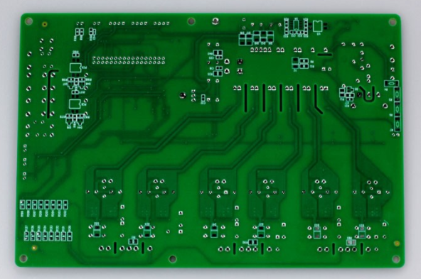
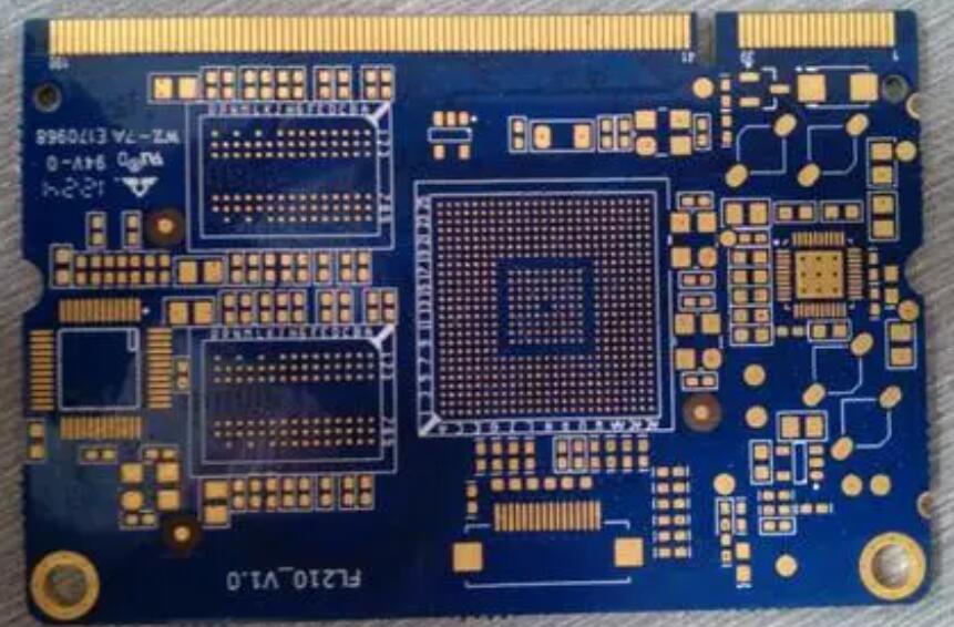
Circuit board proofing: how to deal with vias
1.PCB circuit board plug hole
Standard: The cable hole must be plugged; white light is not allowed (green light is allowed), and the ring shall be processed according to the customer's document. If the ring is covered, part of the via hole is allowed to turn yellow, but the ring is not exposed copper.
Engineering document requirements: plug hole film.
2. Proofing the security through-hole circuit board to cover the plug hole
Standard: The cable hole must be covered and plugged; white light is not allowed (green light is allowed), and the hole is not allowed to turn yellow.
Engineering document requirements: plug hole film.
Proofing production of through-hole circuit boards.
3. Proofing production coverage of security through-hole circuit boards
Standard: The wire hole must be covered with normal silk screen solder mask, no special plug hole treatment; part of the hole is allowed to be plugged, and some holes are not plugged. It must accept the yellowing of the hole, but not the exposed copper of the hole ring.
Engineering document requirements: normal solder mask film.

4. Security through-hole circuit board proofing production is not clogged
Standard: The wire hole must be covered with normal silk screen solder mask, no special plug hole treatment; part of the hole is allowed to be plugged, and some holes are not plugged. It must accept the yellowing of the hole, but not the exposed copper of the hole ring.
Engineering document requirements: normal solder mask film.
5. Cover the pad without covering the hole
Standard: The wire hole must be covered with normal screen printing on the entire board without special plugging treatment; part of the hole is allowed to be plugged, and some holes are not plugged, and the hole ring exposed copper is ±2mil after opening the window according to the customer's document.
Engineering document requirements: normal solder mask film.
6. No coverage
Standard: All cable holes are treated with windows; oil and plug holes are allowed in part of the via holes, but ink on the ring is not allowed.
Engineering document requirements: normal solder mask film.
7. Partial coverage
Standard: The via hole in the designated area must be covered with normal screen printing and no special plugging treatment; part of the via hole in this area is allowed to be plugged, and some holes are not plugged, and the yellowing of the hole must be accepted, but not accepted The hole ring exposes copper.
Engineering document requirements: normal solder mask film.
8. Part of the plug hole
Standard: The via hole in the designated area must be plugged; the via plug hole in this area is not allowed to pass white light (green light is allowed), but it must accept part of the hole opening to yellow, but does not accept the hole ring exposed copper .
Engineering document requirements: plug hole film.
other instructions:
⑴, all PCB circuit boards that need to be plugged, the project must be plugged with film.
⑵. If there is a customer's cable hole that does not allow plugging, the order must be specified in the user order, and the project must be out of the stop film; and this item can only be used for holes above 0.4mm, and holes less than 0.4mm have this requirement. Unconventional processes must be reviewed next time.
iPCB is a high-tech manufacturing enterprise focusing on the development and production of high-precision PCBs. iPCB is happy to be your business partner. Our business goal is to become the most professional prototyping PCB manufacturer in the world. Mainly focus on microwave high frequency PCB, high frequency mixed pressure, ultra-high multi-layer IC testing, from 1+ to 6+ HDI, Anylayer HDI, IC Substrate, IC test board, rigid flexible PCB, ordinary multi-layer FR4 PCB, etc. Products are widely used in industry 4.0, communications, industrial control, digital, power, computers, automobiles, medical, aerospace, instrumentation, Internet of Things and other fields.