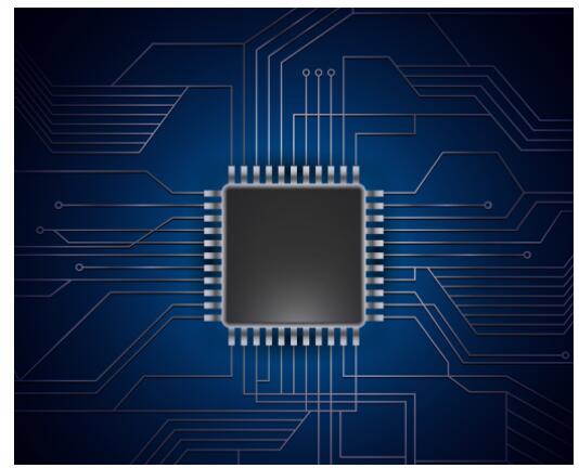
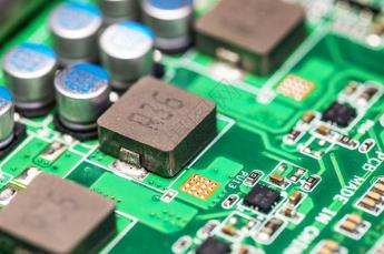
The printed circuit board (PCB) is the core of most electronic products today, and the basic functions are determined by the combination of components and wiring mechanisms. Most PCBs in the past were relatively simple and limited by manufacturing technology, while today's PCBs are much more complicated. From advanced flexible choices to special-shaped varieties, PCBs have become more diverse in today's electronic world. However, multi-layer PCBs are particularly popular.
Although PCBs used for simple electronic devices with limited functions are usually composed of a single layer, more complex electronic devices (such as computer motherboards) are composed of multiple layers. These are the so-called multilayer PCBs. With the increasing complexity of modern electronic devices, these multilayer PCBs are more popular than ever before, and manufacturing technology has significantly reduced their size.
What is a multilayer PCB?
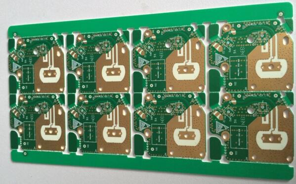
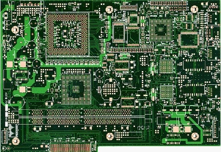
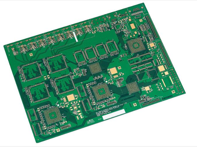
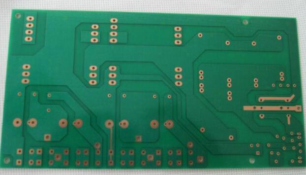
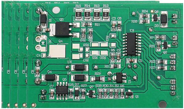
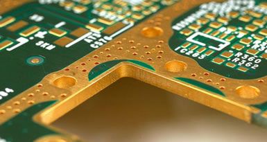
The definition of a multilayer PCB is a PCB made of three or more conductive copper foil layers. They look like several layers of double-sided circuit boards, laminated and glued together, with multiple layers of thermal insulation between them. The entire structure is arranged so that two layers are placed on the surface side of the PCB to connect to the environment. All electrical connections between layers are achieved through through holes such as plated through holes, blind holes and buried holes. Then apply this method to generate highly complex PCBs of different sizes.

The multi-layer PCB has emerged as the times change to the ever-changing changes in the electronics industry. Over time, the functions of electronic devices have gradually become more and more complex, requiring more complex PCBs. Unfortunately, PCBs are limited by problems such as noise, stray capacitance, and crosstalk, and therefore need to follow certain design constraints. These design considerations make it difficult to obtain satisfactory performance from single-sided or even double-sided PCBs-so multilayer PCBs were born. Packaging the power of a double-layer PCB into this format is only a small part of the size, and multilayer PCBs are becoming more and more popular in electronic products. They are available in various sizes and thicknesses to meet the needs of their extended applications, and their variants range from 4 to 12 layers. The number of layers is usually an even number, because an odd number of layers may cause problems in the circuit, such as warpage, and it is not cost-effective to produce. Most applications require 4 to 8 layers, but applications such as mobile devices and smart phones often use about 12 layers, and some professional PCB manufacturers have the ability to produce nearly 100 layers of multilayer PCBs. However, multilayer PCBs with multiple layers are rare because of their extremely low cost efficiency. Although the production of multilayer PCBs is often more expensive and labor-intensive, multilayer PCBs are becoming an important part of modern technology. This is mainly due to the many benefits they provide, especially when compared to single-layer and double-layer varieties.