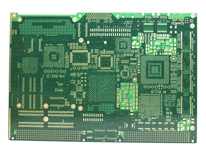
PCB circuit board blind hole board production knowledge
With the development of products in the electronics industry towards high density and high precision, the same requirements have been put forward on circuit boards accordingly. The most effective way to increase the density of the PCB circuit board is to reduce the number of through holes, and to accurately set the blind hole board (PCB circuit board/circuit board) and buried holes to achieve it.
1. Definition of Blind Hole Circuit Board
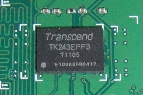
a: In contrast to through holes, through holes refer to holes drilled through each layer, and blind holes are non-drilled through holes. (Illustration, examples of eight-layer board: through holes, blind holes, buried holes) b: Blind hole subdivision: BLIND HOLE, BURIED HOLE (outer layer is not visible); c: From the production process Distinction: Blind holes are drilled before pressing, and through holes are drilled after pressing.

2. Production method
1. Drill belt:
A: Select reference point: Select the through hole (ie a hole in the first drilled belt) as the unit reference hole.
B: Each blind hole drilling belt needs to select a hole, and mark its coordinates relative to the unit reference hole.
C: Pay attention to which drill belt corresponds to which layers: the unit sub-hole diagram and drill bit table must be marked, and the names of the front and back must be the same; the sub-hole diagram cannot be displayed with abc, and the previous one is represented by 1st, 2nd Condition.
Note that when the laser hole is sleeved with the inner buried hole, that is, the holes of the two drill belts are in the same position, you need to ask the customer to move the position of the laser hole to ensure the electrical connection.
2. Production of pnl board edge process hole:
Ordinary multi-layer circuit board: no drilling in the inner layer;
A: Rivets gh, aoi gh, et gh are all shot after eroding the board (beer out)
B: target hole (drilled hole gh) ccd: the outer layer needs to be copper out, x-ray machine: directly punch out, and note that the minimum length of the long side is 11 inches.
Blind hole plate: All tooling holes are drilled, pay attention to rivets gh; need to be out to avoid misalignment. (aoi gh is also a beer), the edge of the pnl board needs to be drilled to distinguish each board.
3. Film modification:
1. Indicate that the film has a positive film and a negative film:
General principle: The board thickness is greater than 8mil (without copper), the positive film process is adopted;
The thickness of the board is less than 8mil (without copper) and the negative film process (thin board);
Line thickness When the line gap valley is large, the copper thickness at d/f should be considered, not the bottom copper thickness.
The blind hole ring can be made 5mil, no need to make 7mil.
The inner independent pad corresponding to the blind hole needs to be retained.
Blind holes cannot be made without ring holes.
Fourth, the process:
The buried-hole board is the same as the common double-sided circuit board.
Blind hole plate, that is, one side is the outer layer:
Positive film process: Single-sided d/f is required, and attention must be paid not to roll the wrong side (when the double-sided bottom copper is inconsistent); when d/f is exposed, the glossy copper surface is covered with black tape to prevent light transmission.
Because the blind hole board is made more than two times, the thickness of the finished product is very easy to be too thick. Therefore, the thickness of the board should be controlled and the range of copper thickness should be indicated after etching.
After pressing the board, use the x-ray machine to punch out the target holes for the multilayer board.
Negative film process: For thin plates (<12mil with copper) because it cannot be produced in the drawing circuit, it must be produced in the water drawing, and the water drawing cannot be divided into two sides, so it can not be made according to the requirements of mi. Small current. If the positive film process is used, the copper thickness on one side is often too thick, causing etching difficulties and the phenomenon of thin lines. Therefore, this type of board needs to use the negative film process.
5. The drilling sequence of through holes and blind holes is different, and the deviation is inconsistent during production
Blind hole plates are more prone to deformation, and it is difficult to open horizontal and straight materials to control multi-layer board alignment and tube spacing. Therefore, only open horizontal or only straight materials when cutting.
Six, Laser drill
LASER DRILL is a kind of blind hole with its own characteristics:
Aperture size: 4-6 mil
pp thickness must be <=4.5mil, calculated according to aspect ratio<=0.75:1
There are three types of pp: LDPP 106 1080; FR4 106 1080; RCC.
Seven, how to define the buried hole plate needs to use resin plug hole
1. H1 (CCL): H2 (PP) 〉=4 thickness ratio
2. HI (CCL) 》32 MIL
3.2OZ and above 2OZ laser buried vias; high-thick copper, high tg boards need to be sealed with resin.
For the boarding process of this type of board, attention should be paid to sealing the hole with resin before making the circuit so as not to cause greater damage to the circuit.
iPCB is a high-tech manufacturing enterprise focusing on the development and production of high-precision PCBs. iPCB is happy to be your business partner. Our business goal is to become the most professional prototyping PCB manufacturer in the world. Mainly focus on microwave high frequency PCB, high frequency mixed pressure, ultra-high multi-layer IC testing, from 1+ to 6+ HDI, Anylayer HDI, IC Substrate, IC test board, rigid flexible PCB, ordinary multi-layer FR4 PCB, etc. Products are widely used in industry 4.0, communications, industrial control, digital, power, computers, automobiles, medical, aerospace, instrumentation, Internet of Things and other fields.