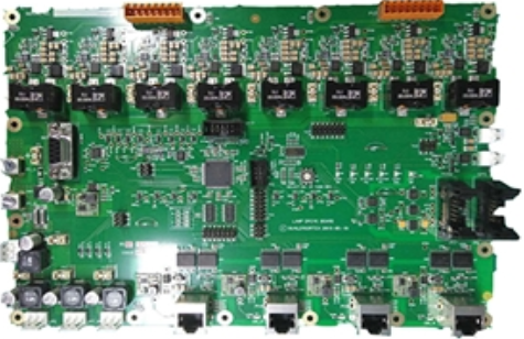
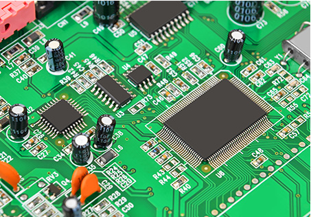
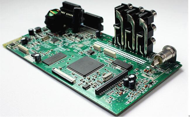
At present, the world of PCB circuit boards is developing rapidly, and the technology also makes the density very high, and the structure and packaging of the small boards allow many components per square inch. Basically, it realizes many technical functions in a small space.
For example,HDI has proven to be invaluable and vital in producing small and compact electronic equipment. As we know, without HDI, mobile phones, laptops, high-speed performance and computers would not be possible.
Examples of HDI technology include fine lines and spaces, sequential lamination, back drilling, non-conductive and conductive via filling, blind vias, buried vias, and microvias. These are especially PCB technologies that allow compact and miniaturized packaging, and Allowing a high level of performance must be accepted and mastered when the cost of manufacturing high-density integrated circuit boards increases to meet the constantly demanding requirements of the electronics industry.

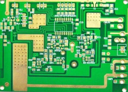
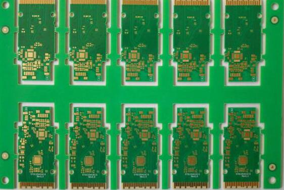
With the rapid development of electronic products, high-density, multi-functional and miniaturization has become the direction of development, but the size of PCB circuit boards continues to decrease. Usually, some small carrier boards are required. If the round holes of the small carrier boards are soldered to the mother board with solder For the circuit board, due to the large volume of the round hole, there will be a problem of virtual soldering, which will make the printed circuit board unable to make a good electrical connection, so a metalized half-hole plate appears. The characteristics of the metalized half-hole plate are: individual Smaller, there are a whole row of metalized half-holes on the side of the unit, through which the metalized half-holes and the pins of the components are welded together.
PCB half-hole board processing difficulties:
After the PCB half-hole board is formed, the copper skin of the hole wall is blackened, burrs are left, etc., which have always been a problem in the molding process of various PCB manufacturers, especially the whole row of half holes. The general metallized half-hole plate forming processing methods include CNC milling machine gongs, mechanical punching punching, VCUT cutting, etc. These processing methods will result in the remaining part of the PTH hole section when removing the unnecessary part of the hole to make copper.
Copper wires and burrs are left, and the copper skin of the hole wall may be lifted and peeled off in serious cases. On the other hand, when the metallized half-hole is formed, due to PCB expansion and contraction, drilling hole position accuracy, and forming accuracy, the size of the remaining half-holes on the left and right sides of the same unit is large during the forming process, which brings customers welding and assembly. Greatly troubled.