Surface mount IC packages rely on printed circuit boards for heat dissipation. In general, PCBs are the primary cooling method for high-power semiconductor devices. A good PCB thermal design has a huge impact, it can keep the system running well, and it can also bury the hidden danger of thermal accidents. Careful handling of PCB layout, board construction, and device placement can help improve thermal performance in mid- to high-power applications.

Semiconductor manufacturing companies have difficulty controlling the systems in which their devices are used. However, the system in which the IC is mounted is critical to overall device performance. For custom IC devices, the system designer often works closely with the manufacturer to ensure that the system meets the many thermal requirements of high-power devices. This early collaboration ensures that the IC meets electrical and performance standards while maintaining proper operation within the customer's cooling system. Many large semiconductor companies sell their devices as standard parts, with no contact between the manufacturer and the end application. In this case, we can only use some general guidelines to help achieve a better passive cooling solution for IC and systems.
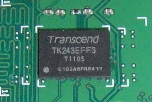
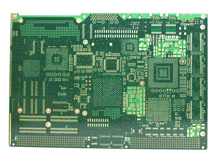
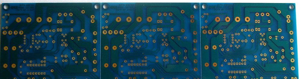
Common semiconductor package types are exposed pad or PowerPADTM style packages. In these packages, the chip is attached to a piece of metal called a die pad. This chip pad supports the chip during chip processing and is also a good thermal path for heat dissipation of the device. When the exposed pad of the package is soldered to the PCB, heat can quickly dissipate from the package and into the PCB. After that, the heat is dissipated through the various PCB layers and into the surrounding air. Exposed-pad packages typically conduct about 80% of the heat that enters the PCB through the bottom of the package. The remaining 20% is dissipated through the device wires and all sides of the package. Less than 1% of the heat is dissipated through the top of the package. For these exposed pad packages, good PCB thermal design is critical to ensure certain device performance.
One aspect of PCB design that can improve thermal performance is PCB device layout. Whenever possible, high-power components on the PCB should be separated from each other. This physical separation between high-power components allows for PCB area around each high-power component to help achieve better heat transfer. Care should be taken to isolate temperature sensitive components from high power dissipation components on the PCB. Whenever possible, high-power components should be mounted away from the corners of the PCB. A more central PCB location allows the board area around power-hungry components to be minimized to help dissipate heat.
The second aspect is the structure of the PCB, an aspect that has a decisive influence on the thermal performance of the PCB design. The general rule is that the more copper the PCB has, the better the thermal performance of the system components. The ideal heat dissipation situation for semiconductor devices is when the die is mounted on a large piece of liquid cooled copper. For most applications, this placement method is not practical, so we can only make some other changes to the PCB to improve thermal performance. For most applications today, overall system size is shrinking, adversely affecting thermal performance. The larger the PCB, the larger the area available for heat conduction, and the greater flexibility to leave enough space between high-power components.
Whenever possible, optimize the number and thickness of PCB copper ground planes. Ground plane copper is generally heavy in weight, and it is an excellent thermal path for heat dissipation throughout the PCB. Arranging the wiring for each layer also increases the overall proportion of copper used for heat conduction. However, this routing is usually done in electrical and thermal isolation, limiting its role as a potential heat sink. The device ground plane should be routed as electrically as many ground planes as possible to aid in thermal conduction. Thermal vias on the PCB below the semiconductor device help heat to enter the buried layers of the PCB and conduct to the back of the board.
The top and bottom layers of a PCB are the "golden ground" for improving thermal performance. Using wider wires, routed away from high-power devices, can provide a thermal path for heat dissipation. Dedicated thermal pads are an excellent way to dissipate heat from a PCB. Thermal pads are typically located on the top or back of the PCB and are thermally connected to the device through direct copper connections or thermal vias. In the case of inline packages (packages with leads on both sides only), this thermal pad can be located on the top of the PCB, shaped like a "dog bone" (the middle is as narrow as the package, and the connection copper area away from the package is larger. large, small in the middle and large at both ends). In the case of a four-sided package (with leads on all four sides), the thermal pad must be on the back of the PCB or into the PCB.
Increasing the thermal pad size is an excellent way to improve the thermal performance of a PowerPAD-style package. Different thermally conductive plate sizes have a dramatic effect on thermal performance. Product data sheets provided in tabular form typically list these dimensions. However, it is difficult to quantify the impact of the added copper of a custom PCB. Using some online calculators, the user can select a device and then change the size of the copper pads to estimate its impact on the thermal performance of a non-JEDEC PCB. These calculation tools highlight the extent to which PCB design affects thermal performance. For a four-sided package, the top pad area is just smaller than the exposed pad area of the device, in which case a buried or backside layer is the first way to achieve better cooling. For dual in-line packages, we can use a "dog bone" pad pattern to dissipate heat. Some of the screws used to mount the PCB can also be an effective thermal path to the base of the system where the screws are thermally connected to the thermal pad and ground plane. The number of screws should be a value that reaches the point of diminishing returns, considering thermal conductivity and cost. The metal PCB stiffener has more cooling area after being attached to the thermally conductive plate. For some applications where the PCB is covered with an enclosure, the profiled solder fillet has higher thermal performance than an air-cooled enclosure. Cooling solutions such as fans and heat sinks are also common methods of system cooling, but they often require more space or require design modifications to optimize cooling. To design a system with high thermal performance, it is not enough to choose a good IC device and a closed solution. The thermal performance scheduling of an IC depends on PCB board and the ability of the cooling system to cool the IC device quickly. Using the above passive cooling method, the heat dissipation performance of the system can be greatly improved.