HDI technology is developing rapidly in the field of printed circuit board. This technology allows denser and smaller board structures and packaging, allowing more components per square inch. Basically, it has more technical functions in less space. Facts have proved that HDI is invaluable and critical in producing smaller and more compact electronic equipment. As we know today, without HDI, mobile phones, laptops, and high-speed performance and computing would not be possible.

Examples of HDI technology include fine lines and spaces, sequential lamination, post-drilling, non-conductive and conductive via filling, blind vias, buried vias, and microvias. These are specialized printed circuit board technologies that allow for tight and micro packaging. They also allow higher levels of performance such as controlled impedance and satellite technology.

Manufacturing high-density integrated circuit board brings higher costs, but it must be accepted and mastered in order to meet the increasingly demanding requirements of the electronics industry.
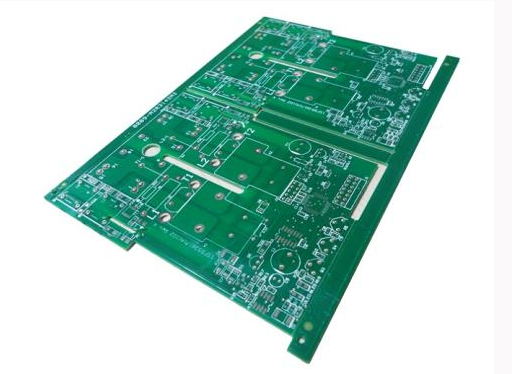
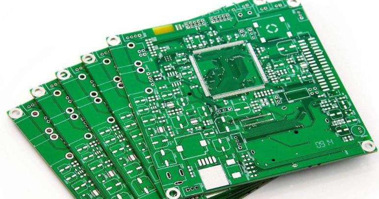
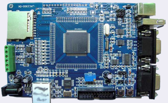
HDI PCB boards are widely used in server HDI cards, mobile phones, multi-function POS machines, and HDI security cameras. What kind of circuit board is HDI PCB board? What is the difference between PCB and regular PCB?
1. What is an HDI PCB board?
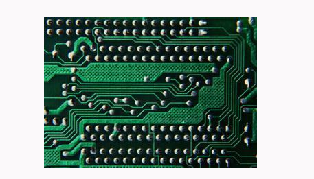
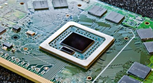
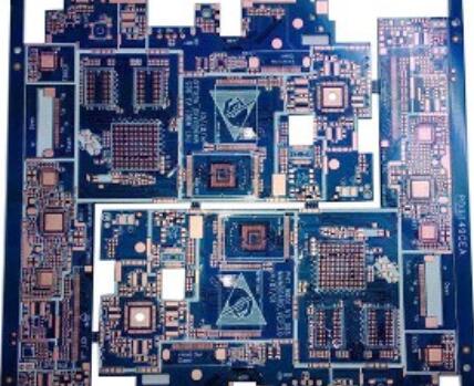
HDI PCB (High Density Interconnector), or High Density Interconnector, is a circuit board with high line distribution density using micro-blind buried hole technology. HDI PCB boards have internal and external lines, which are connected internally by drilling holes and metallization inside holes.
2. Difference between HDI PCB board and normal PCB
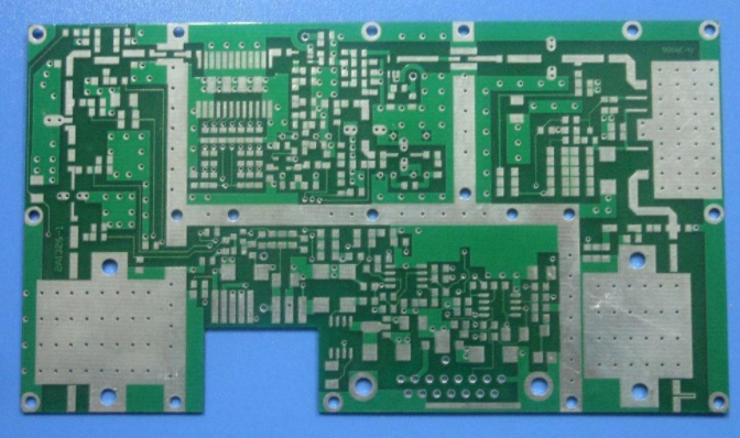
HDI PCB boards are usually manufactured by stacking method. The more times the HDI PCB boards are stacked, the higher the technical grade of the boards. Ordinary HDI PCB board is basically a single layer, high-order HDI uses two or more layers technology, and advanced PCB technology such as stacking, electroplating filling, laser direct drilling, etc. When the density of PCB increases beyond eight layers, it will be cheaper to manufacture with HDI than the traditional complex bonding process.
HDI PCB boards have higher electrical performance and signal correctness than traditional PCBs. In addition, HDI PCB boards have better improvement on radio frequency interference, electromagnetic wave interference, electrostatic discharge, heat conduction, etc. High Density Integration (HDI) technology enables the design of terminal products to be more compact while meeting higher standards for electronic performance and efficiency.
HDI PCB plates are plated with blind holes and then bonded twice, which can be divided into first, second, third, fourth and fifth order. The first order is simple and the process and process are well controlled. The main problems of the second order are the alignment problem and the drilling and copper plating problem. There are many second-order designs, one is the staggered positions of each order, which is equivalent to two first-order HDIs in that the secondary adjacent layer needs to be connected through a wire in the middle layer. The second is that the two first-order holes overlap, and the second-order is achieved by overlapping. The processing is similar to the two first-order, but there are a lot of process essentials to be specially controlled, which is mentioned above. The third is to punch directly from the outer layer to the third layer (or N-2 layer), which is different from the previous process and more difficult to punch. For the third order, the second order analogy is yes.
HDI PCB is expensive, so ordinary PCB manufacturers are unwilling to do it. IPCB can be used as HDI blindly buried PCB board that others do not want to do.