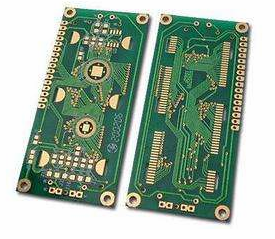
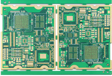
Analysis on the Process of Resin Plug Hole of PCB Circuit Board
1. Via in pad process:
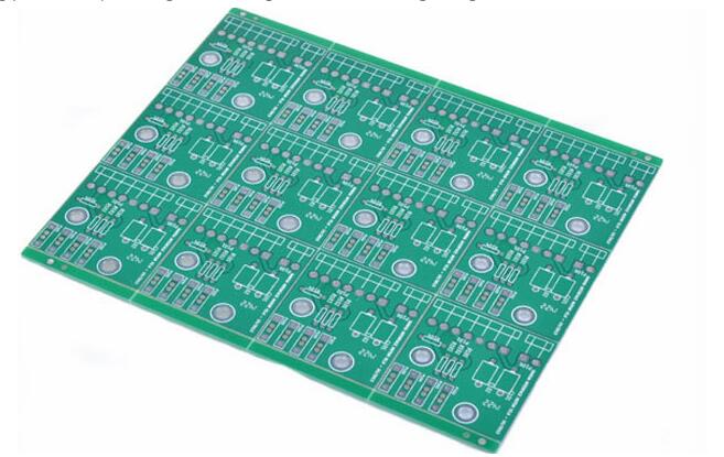
PCB circuit board resin plug hole process
1. Definition
For ordinary PCB boards with small holes and parts to be soldered, the traditional production method is to drill a through hole on the board, and then plate a layer of copper in the through hole to realize the conduction between layers, and then Lead out a wire to connect to a pad to complete the welding with external parts.
2. Development
Nowadays, circuit boards are becoming more and more high-density and interconnected. There is no more space to place these through-hole wires and pads. Therefore, in this context, the production process of Via in pad has emerged.
3. Function
Via in pad's production process makes the circuit board production process three-dimensional, effectively saving horizontal space, and adapting to the development trend of modern circuit boards with high density and interconnection.

2. Traditional resin plugging process
1. Definition
The resin plugging process refers to the use of resin to plug the buried holes of the inner layer, and then pressure bonding, which is widely used in high-frequency boards and HDI boards; it is divided into traditional silk screen resin plug holes and vacuum resin plug holes. The general product manufacturing process is traditional silk-screen resin plugging, which is also the most commonly used process method in the industry.
2. Process
Pre-process-drilling resin hole-electroplating-resin plug hole-ceramic grinding plate-drilling through hole-electroplating-post process
3. Post-process ceramic grinding plate requirements:
(1) Grind each board horizontally and vertically to ensure that the resin on the surface of the board is cleaned, and the resin can be repaired by hand polishing if the part is not cleaned;
(2) The resin recess after grinding the board should not be greater than 0.075mm.
4. Electroplating requirements:
Electroplating is carried out according to the customer's copper thickness requirements. After electroplating, perform slicing to confirm the recession of the resin plug hole.
Three: Vacuum resin plugging process
1. Definition
The vacuum silk screen plugging machine is a special equipment manufactured for the PCB industry. The equipment is suitable for PCB blind hole resin plug holes, small hole resin plug holes, and small hole thick plate resin plug holes. In order to ensure that the resin plug hole is printed without air bubbles, the equipment is designed and manufactured with high vacuum, and the absolute vacuum value of the vacuum chamber is below 50Pa. At the same time, the vacuum system and screen printing machine adopt anti-vibration and high-strength designs to make the equipment run more stable.
2. The difference
The vacuum plugging process is similar to the traditional screen printing plugging process. The difference is that during the plugging process, the product is in a vacuum state, which can effectively reduce defects such as bubbles.
3. Production process
Aluminum sheet--open oil--vacuum ink--install screen pad--align--vacuum equipment--test printing--inspection--mass production--segment curing--ceramic grinding plate
iPCB is a high-tech manufacturing enterprise focusing on the development and production of high-precision PCBs. iPCB is happy to be your business partner. Our business goal is to become the most professional prototyping PCB manufacturer in the world. Mainly focus on microwave high frequency PCB, high frequency mixed pressure, ultra-high multi-layer IC testing, from 1+ to 6+ HDI, Anylayer HDI, IC Substrate, IC test board, rigid flexible PCB, ordinary multi-layer FR4 PCB, etc. Products are widely used in industry 4.0, communications, industrial control, digital, power, computers, automobiles, medical, aerospace, instrumentation, Internet of Things and other fields.