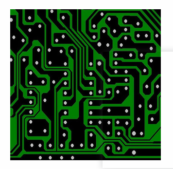
Wiring rules and skills of multi-layer PCB circuit boards
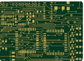
High-frequency circuit board design is a particularly complex design process, and its wiring is very important for the entire design! With the continuous development and progress of electronic technology, large-scale and high-precision PCB circuit boards have been widely used, and the components are in The mounting density of printed circuit boards is becoming higher and higher. Simple single-sided and double-sided wiring can no longer meet the requirements of high-performance circuits, so multilayer PCB circuit boards are required for wiring.
High-frequency circuits often have relatively high integration and high wiring density. Showing off multi-layer boards is not only necessary for wiring, but also an effective means to reduce interference. In the PCB Layout stage, a reasonable selection of the printed board size with a certain number of layers can make full use of the intermediate layer to set the shielding, better realize the nearest grounding, and at the same time can more effectively reduce the parasitic inductance and shorten the signal transmission length, and It can also reduce signal cross-interference to a large extent, and all these methods are beneficial to the reliability of high-frequency circuits.

More than 1, 3 points, it is best to make the line pass through each point in sequence, which is convenient for testing, and the line length is best to be short.
2. The lines between different layers are best not to be parallel to avoid actual capacitance.
3. It is best not to put wires between the pins, especially between and around the pins of integrated circuits.
4. The wiring should be as straight as possible, or a 45-degree polyline, to prevent electromagnetic radiation.
5. It is best to keep the lines neatly between the lines, and it is best to connect the ground polylines together to enlarge the grounding area.
6. Pay attention to the discharge of components more evenly, which is convenient for installation, plug-in, welding and other operations. The characters are arranged in the current character layer, the position is reasonable, pay attention to the orientation, to prevent being blocked, and it is also convenient for production.
7. Consider the structure of component placement. SMD components with positive and negative poles should be marked at the package and at the end to prevent space conflicts.
8. It is best to put the functional block components together, and the zebra strips and other components near the LCD should not be too close.
9. After the wiring is completed, carefully check whether each wire is really connected (the lighting method can be used).
iPCB is a high-tech manufacturing enterprise focusing on the development and production of high-precision PCBs. iPCB is happy to be your business partner. Our business goal is to become the most professional prototyping PCB manufacturer in the world. Mainly focus on microwave high frequency PCB, high frequency mixed pressure, ultra-high multi-layer IC testing, from 1+ to 6+ HDI, Anylayer HDI, IC Substrate, IC test board, rigid flexible PCB, ordinary multi-layer FR4 PCB, etc. Products are widely used in industry 4.0, communications, industrial control, digital, power, computers, automobiles, medical, aerospace, instrumentation, Internet of Things and other fields.