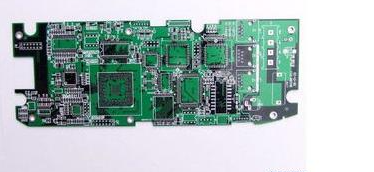
In the PCB design of electronic system, in order to avoid detours and save time, we should fully consider and meet the requirements of anti-interference, and avoid anti-interference remedial measures after the design is completed. There are three basic elements to form interference:
(1) An interference source refers to an interference component, device, or signal, which is described in mathematical la
nguage as follows: DU /dt, DI /dt An interference source is large. Such as: lightning, relay, thyristor, motor, high frequency clock, etc., can become an interference source.

(2) Propagation path: refers to the path or medium through which the interference spreads from the interference source to the sensitive device. The typical interference propagation paths are conduction through wires and radiation in space.
(3) Sensitive devices refer to objects easily disturbed. Such as: A/D, D/A converter, MCU, digital IC, weak signal amplifier, etc. The basic principle of anti-interference design is to suppress the interference source, cut off the interference propagation path, and improve the anti-interference performance of sensitive devices.
1 Suppress interference sources
To suppress an interference source, minimize the DU /dt and di/dt of the interference source. This is the first consideration and important principle in anti-interference design, often can get twice the result with half the effort. To reduce the DU/DT of an interference source, connect capacitors in parallel at both ends of the interference source. To reduce the DI/DT of the interference source, the inductor or resistor is connected in series in the interference source circuit and the continuous diode is added.
Common measures to suppress interference sources are as follows:
(1) Continuous diode is added to relay coil to eliminate the back emf interference generated when the coil is disconnected. Adding only the continuous diode will make the disconnect time of the relay lag, and the relay can operate more times per unit time after adding the regulated diode.
(2) Spark suppression circuit is connected at both ends of relay contact (RC series circuit in general, resistance is usually selected from several K to dozens of K, capacitance is selected from 0.01uF) to reduce the impact of electric spark.
(3) Add filter circuit to motor, pay attention to capacitor and inductor leads should be as short as possible.
(4) Each IC on the circuit board should be connected with a 0.01μF ~ 0.1μF high frequency capacitor to reduce the influence of IC on the power supply. Pay attention to the wiring of high-frequency capacitors. The wiring should be close to the power supply end and as short as possible. Otherwise, the equivalent series resistance of the capacitance will be increased, which will affect the filtering effect.
(5) Avoid 90 degree broken line when wiring, reduce high-frequency noise emission.
(6) both ends of the SCR and RC suppression circuit, reduce the noise generated by the SCR (this noise may be serious when the SCR breakdown).
According to the propagation path of interference, it can be divided into two types: conduction interference and radiation interference.
The so-called conducted interference refers to the interference transmitted to the sensitive device through the wire. The h
igh-frequency noise is different from the useful signal in frequency band. It can be cut off by adding filters on the wire, and sometimes it can also be solved by adding isolated optical coupler. Power supply noise hazards, to pay special attention to treatment. The so-called radiation interference refers to the interference propagated to sensitive devices through space radiation. The general solution is to increase the distance between the interference source and the sensitive device, isolate them by the ground line and add a cover on the sensitive device.
2 Common measures to cut off the interference propagation path are as follows:
(1) Fully consider the influence of power supply on SCM. If the power supply is done well, the anti-interference of the whole circuit is solved for the most part. Many microcontroller is very sensitive to the noise of the power supply, so it is necessary to add a filter circuit or a voltage regulator to the power supply to reduce the interference of the noise of the power supply to the single chip. For example, magnetic beads and capacitors can be used to form a π -shaped filter circuit, but less demanding conditions can also be replaced by 100 ω resistors.
(2) if the I/O port of MCU is used to control noise devices such as motors, isolation should be added between the I/O port and the noise source (increase π -shaped filter circuit). Control motor and other noise devices, in the I/O port and noise source should be isolated (increase π -shaped filter circuit).
(3) Pay attention to crystal wiring. Crystal oscillator and MCU pin as close as possible, the ground line to the clock area isolated, crystal oscillator shell grounded and fixed. This measure will solve many difficult problems.
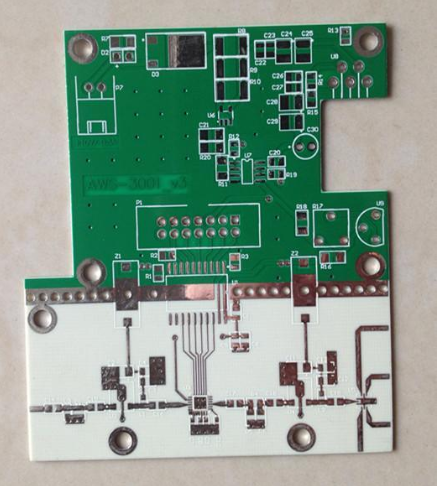
(4) reasonable partition of the circuit board, such as strong and weak signals, digital and analog signals. Keep interference sources (such as motors and relays) away from sensitive components (such as microcontrollers) as far as possible.
(5) The ground line separates the digital area from the analog area. The digital ground and the analog ground should be separated and connected to the power supply ground at one point. The wiring of A/D and D/A chips is also based on this principle. The manufacturer has taken this requirement into account when assigning pin arrangement of A/D and D/A chips.
(6) The ground wire of MCU and high-power device should be separately grounded to reduce mutual interference. High-power components should be placed at the edge of the circuit board whenever possible.
(7) In the MCU I/O port, power line, circuit board connection line and other key places to use anti-interference components such as magnetic beads, magnetic rings, power filters, shielding cover, can significantly improve the anti-interference performance of the circuit.
Improve the anti-interference performance of sensitive devices
Improving the anti-interference performance of sensitive devices refers to the method of reducing the pick up of interference noise and recovering from abnormal state as soon as possible.
Common measures to improve the anti-interference performance of sensitive devices are as follows:
(1) When wiring, minimize the area of loop ring to reduce the induced noise.
(2) When wiring, power cables and ground cables should be as thick as possible. In addition to reducing the pressure drop, it is more important to reduce coupling noise.
(3) For the IDLE I/O port of the MCU, do not hang, to ground or connect to the power supply. Idle ends of other ics are grounded or connected to power without changing system logic.
(4) The use of power monitoring and watchdog circuit for single chip microcomputer, such as IMP809, IMP706, IMP813, X25043, X25045, etc., can greatly improve the anti-interference performance of the whole circuit.
(5) On the premise that the speed can meet the requirements, try to reduce the crystal vibration of the single chip and select low speed digital circuit.
(6) IC devices as far as possible directly welded on the circuit board, with less IC seat.
In order to achieve a good anti-interference, so we often see the PCB board on the ground division of the wiring. But not all hybrid digital and analog circuits must be ground - plane split. Because such segmentation is to reduce the interference of noise.
Theory: general frequency in digital circuit will be higher than the frequency of analog circuit, and they themselves will signal with ground plane form a reflux (because in signal transmission, copper wire and copper wire exists between all kinds of distributed capacitance and inductance), if we put the ground mixed together, then the backflow will mutually crosstalk in the digital and analog circuits. And we separate them so that they form a reflux only within themselves. They're only connected by a zero ohmic resistor or a magnetic bead because they were the same physical ground, and now the wiring separates them, and they should be connected.