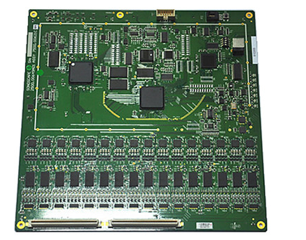
PCB double-sided circuit layout is particularly particular
PCB board is also called printed circuit board and printed circuit board. In short, it is a thin board on which integrated circuits and other electronic components are placed. Anyone who knows a little about circuit boards knows that there are single-panel, double-panel, and multi-layer boards according to their classification. Let's focus on the little-known points of double-panel grounding.
What is a double-sided PCB? In fact, the double-sided board is an extension of the single-sided board. Strictly speaking, the double-sided board is a very important PCB board in the circuit board. Another important feature of the double-sided board is that there are through holes, that is, the copper foil layers cannot communicate with each other, and an insulating layer is laid between each layer of copper foil, so they need to rely on the through holes to carry out Signal link, so it has the title of via. Because the area of the double-sided board is twice as large as that of the single-sided board, and because the wiring can be interleaved (it can be wound to the other side), it is more suitable for use in circuits that are more complicated than the single-sided board.

When designing printed circuit boards, automatic wiring is often used. Usually, pure digital circuit boards, especially with low signal levels and low circuit density, are no problem with automatic wiring. However, when designing analog, mixed-signal or high-speed circuit boards, if the automatic routing tools of the routing software are used, some problems may occur, and it may even cause serious circuit performance problems.
In addition, when using manual wiring, pay attention to the following requirements to ensure good results:
1. Design the grounding as a ground plane as the current return path.
2. Separate the analog ground plane from the digital ground plane.
3. If it is unavoidable that the signal wires and the ground are placed on the same layer, design the signal wires and the ground wires to be perpendicular to each other to reduce the interference caused by the signal wires to the ground current loop.
4. Place the analog circuit next to the circuit board, and place the digital circuit system closest to the power supply. It can reduce the impact of digital switching δi/δt on analog circuits.
Therefore, a single-sided PCB circuit board cannot design complex circuits, while a double-sided PCB and a multi-sided PCB are different, and complex circuit designs can be performed. There are wiring on both sides of the double-sided board, but if you want to use the wires on both sides, you must have a proper circuit connection between the two sides. This kind of bridge between circuits is called a via. A via is a small hole filled or coated with metal on the PCB, which can be connected with the wires on both sides. The above is the knowledge points that the editor of PCB factory wants to tell you today, I hope it can help you.