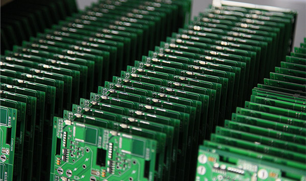
Analysis of the bubble generated by infrared heat melting of PCB multilayer printed circuit board
In the pattern electroplating process method, the printed circuit board generally uses the tin-lead alloy layer, which is not only used as a pattern metal corrosion layer, but also provides a protective layer and a solder layer for the lead-tin board. Because of the pattern plating-etching process, after the circuit pattern is etched, both sides of the wire are still copper layers, which are prone to contact with air to produce an oxide layer or be corroded by acid and alkali media.
In addition, since the circuit pattern is prone to undercut during the etching process, the tin-lead alloy plating part is suspended and a suspension layer is generated. But it is easy to fall off, causing short circuit between wires. The use of infrared hot melt technology can make the exposed copper surface get extremely good protection. At the same time, the tin-lead alloy coating on the surface and in the hole can be recrystallized after infrared heat melting, making the metal surface shiny. It not only improves the solderability of the connection point, but also ensures the reliability of the connection between the components and the inner and outer layers of the circuit. However, when used for infrared heat melting of multilayer printed circuit boards, due to the high temperature, the delamination and blistering between layers of the multilayer printed circuit board is very serious, which results in the finished product of the multilayer printed circuit board. The rate is extremely low.

What causes the quality problem of layered blistering of multilayer printed circuit board? Research on the recurrence mechanism of quality problems based on the data obtained from multiple experiments. At first, it was only analyzed from the lamination process. It was believed that the gas was not completely driven out during the lamination process. However, due to the higher temperature during the heat melting, the gas expansion produces a larger outward pushing force. When the resulting pushing force is greater than the interlayer The bonding strength sometimes produces delamination and blistering. According to the results of the analysis, samples of prepregs with different storage conditions are sampled, and then pressure tests are carried out under different temperature conditions. As a result, after infrared heat fusion, the layered blisters were still formed, and the phenomenon was similar to that of laminated multilayer printed circuit boards. It also analyzes and studies the surface pretreatment, especially the strengthening of the surface of the bonded copper foil, and the roughening treatment of the copper foil to increase the contact surface area with the prepreg, so that the prepreg has a better surface than the oxidized copper foil. Great bond strength.
iPCB is happy to be your business partner. Our business goal is to become the most professional prototyping PCB manufacturer in the world. With more than ten years of experience in this field, we are committed to meeting the needs of customers from different industries in terms of quality, delivery, cost-effectiveness and any other demanding requirements. As one of the most experienced PCB manufacturers and SMT assemblers in China, we are proud to be your best business partner and good friend in all aspects of your PCBneeds. We strive to make your research and development work easy and worry-free.
quality assurance
iPCB has passed ISO9001:2008, ISO14001, UL, CQC and other quality management system certifications, produces standardized and qualified PCB products, masters complex process technology, and uses professional equipment such as AOI and Flying Probe to control production and X-ray inspection machines. Finally, we will use double FQC inspection of appearance to ensure shipment under IPC II standard or IPC III standard.